Market Trends
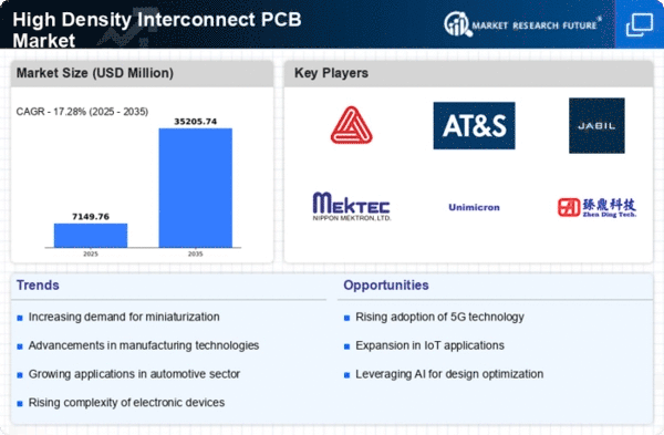
Key Emerging Trends in the High Density Interconnect PCB Market
As electronic devices become more intricate and compact, the size and aspect ratio of vias, along with component density, are also decreasing. Multilayer PCB boards with traces as small as 3mil (0.075mm) now feature a higher concentration of microvias. These microvias play a crucial role in creating high-density interconnects (HDI) for printed circuit boards (PCBs).
PCB manufacturers are generally capable of drilling via holes as small as 6 mils (0.15mm), but mechanical drilling can be costly due to tooling expenses. The thin drills used in this process are prone to breakage, especially for microvias with a high aspect ratio.
HDI PCBs are commonly found in complex electronic devices that demand exceptional performance while maintaining a compact form factor. Applications include mobile phones, touch-screen devices, laptop computers, digital cameras, 4/5G network communications, and military applications such as avionics and smart munitions.
The automotive and aerospace industries, where lower weight translates into more efficient operation, have increasingly embraced HDI PCBs. HDI PCBs are also prominent in medical devices; advanced electronic medical devices, such as equipment for monitoring, imaging, surgical procedures, and laboratory analysis, incorporate HDI boards. With high-density technology, monitoring and medical testing could become more accurate and more cost-effective.
The growing sophistication of industrial automation has led to the widespread adoption of IoT devices in manufacturing, warehousing, and other industrial settings. HDI technology is integral to many of these advanced pieces of equipment. Businesses today rely on electronic tools to track inventory and monitor equipment performance. Machines are increasingly equipped with smart sensors that collect usage data and communicate with other smart devices, providing valuable insights to optimize operations.
Similar to other advancements, cars are becoming more connected and computerized. Most modern cars have around 50 microprocessors, responsible for engine control, diagnostics, safety features, and various other tasks. Numerous advanced features, including onboard Wi-Fi, GPS, rearview cameras, and backup sensors, depend on HDI PCBs. As automotive technology continues to evolve, HDI technology is likely to play an increasingly significant role.
Beyond medical devices, HDI PCBs are extensively used in equipment for monitoring, imaging, surgical procedures, laboratory analysis, and more. The utilization of high-density technology could enhance the accuracy and cost-effectiveness of monitoring and medical testing.
In summary, HDI PCBs have emerged as a transformative technology, revolutionizing the design and manufacturing of electronic devices. Their ability to pack more circuitry into a smaller space, coupled with their enhanced reliability and signal integrity, makes them the preferred choice for engineers, designers, and manufacturers alike.


Leave a Comment