• Cat-intel
  • MedIntelliX
  • Resources
  • About Us
  • Request Free Sample ×

    Kindly complete the form below to receive a free sample of this Report

    Leading companies partner with us for data-driven Insights

    clients tt-cursor
    Hero Background

    Wafer Level Test Burn In Market

    ID: MRFR/PNT/22367-HCR
    111 Pages
    Snehal Singh
    October 2025

    Wafer Level Test And Burn In Wltbi Market Research Report By Technology (Electrical Test (e-test), Burn-In Test, Optical Inspection), By Application (Semiconductors, Integrated Circuits (ICs), Microprocessors, Memory Devices), By End-Use Industry (Automotive, Consumer Electronics, Industrial, Aerospace & Defense), By Form Factor (Wafer-Level, Package-Level, Die-Level), By Test Type (Functional Test, Parametric Test, Reliability Test) and By Regional (North America, Europe, South America, Asia Pacific, Middle East and Africa) - Forecast t...

    Share:
    Download PDF ×

    We do not share your information with anyone. However, we may send you emails based on your report interest from time to time. You may contact us at any time to opt-out.

    Wafer Level Test Burn In Market Infographic
    Purchase Options

    Wafer Level Test Burn In Market Summary

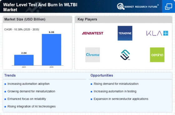
    As per MRFR analysis, the Wafer Level Test And Burn In WLTBI Market Size was estimated at 2.044 USD Billion in 2024. The WLTBI industry is projected to grow from 2.257 USD Billion in 2025 to 6.059 USD Billion by 2035, exhibiting a compound annual growth rate (CAGR) of 10.38 during the forecast period 2025 - 2035.

    Key Market Trends & Highlights

    The Wafer Level Test And Burn In (WLTBI) Market is poised for substantial growth driven by technological advancements and increasing demand for efficiency.

    • The integration of advanced testing technologies is reshaping the WLTBI landscape, particularly in North America, which remains the largest market.
    • Automation and efficiency are becoming focal points in the WLTBI sector, enhancing operational capabilities across various applications.
    • The rising demand for energy-efficient solutions is particularly evident in the semiconductor segment, which continues to dominate the market.
    • Key market drivers include the growing adoption of 5G technology and the emergence of Internet of Things (IoT) devices, significantly impacting both the electrical test and burn-in test segments.

    Market Size & Forecast

    2024 Market Size 2.044 (USD Billion)
    2035 Market Size 6.059 (USD Billion)
    CAGR (2025 - 2035) 10.38%

    Major Players

    Advantest Corporation (JP), Teradyne Inc. (US), KLA Corporation (US), Chroma ATE Inc. (TW), FormFactor Inc. (US), Aetina Corporation (TW), Cohu Inc. (US), SUSS MicroTec SE (DE)

    Wafer Level Test Burn In Market Trends

    The Wafer Level Test And Burn In WLTBI Market is currently experiencing notable growth, driven by the increasing demand for advanced semiconductor technologies. As electronic devices become more sophisticated, the need for efficient testing and reliability assurance has intensified. This market encompasses various processes that ensure the performance and durability of semiconductor wafers, which are critical components in modern electronics. The integration of innovative testing methodologies and automation is reshaping the landscape, allowing manufacturers to enhance yield rates and reduce time-to-market. Furthermore, the rise of Internet of Things (IoT) applications and artificial intelligence (AI) is propelling the need for robust testing solutions, as these technologies require high-performance chips that can withstand rigorous operational conditions. In addition, the Wafer Level Test And Burn In WLTBI Market is witnessing a shift towards miniaturization and increased functionality in semiconductor devices. This trend necessitates more sophisticated testing techniques to ensure that smaller, more complex chips meet stringent quality standards. As manufacturers strive to optimize their production processes, the adoption of advanced testing equipment and methodologies is likely to become more prevalent. The ongoing evolution of the semiconductor industry, coupled with the growing emphasis on energy efficiency and sustainability, suggests that the Wafer Level Test And Burn In WLTBI Market will continue to expand, presenting opportunities for innovation and investment in the coming years.

    Integration of Advanced Testing Technologies

    The Wafer Level Test And Burn In WLTBI Market is increasingly integrating advanced testing technologies to enhance efficiency and accuracy. This trend reflects the industry's response to the growing complexity of semiconductor devices, necessitating more sophisticated testing methods to ensure reliability.

    Focus on Automation and Efficiency

    There is a marked focus on automation within the Wafer Level Test And Burn In WLTBI Market, as manufacturers seek to streamline processes and reduce operational costs. Automation not only improves testing speed but also minimizes human error, contributing to higher quality outcomes.

    Rising Demand for Energy-Efficient Solutions

    The demand for energy-efficient solutions is rising within the Wafer Level Test And Burn In WLTBI Market, driven by global sustainability initiatives. Manufacturers are increasingly prioritizing the development of testing methods that support the production of energy-efficient semiconductor devices.

    The ongoing advancements in semiconductor technology and the increasing demand for miniaturization in electronic devices are driving the evolution of Wafer Level Test and Burn In processes, which are essential for ensuring product reliability and performance.

    U.S. Department of Commerce

    Wafer Level Test Burn In Market Drivers

    Growing Adoption of 5G Technology

    The growing adoption of 5G technology is significantly impacting the Wafer Level Test And Burn In WLTBI Market. As telecommunications companies roll out 5G networks, there is an escalating demand for advanced semiconductor devices that can support higher data rates and lower latency. This surge in demand necessitates rigorous testing and burn-in processes to ensure device reliability and performance. The market for 5G-related semiconductor testing is projected to expand rapidly, with estimates suggesting a growth rate of over 20% annually. Consequently, the need for effective Wafer Level Test And Burn In solutions is becoming increasingly critical, positioning this driver as a key factor in the Wafer Level Test And Burn In WLTBI Market.

    Focus on Automation and Efficiency

    In the Wafer Level Test And Burn In WLTBI Market, there is a pronounced focus on automation and efficiency. Manufacturers are increasingly adopting automated testing solutions to streamline operations and minimize human error. This shift is largely influenced by the need to reduce operational costs while maintaining high-quality standards. Automation technologies, such as robotics and automated test equipment, are being integrated into testing processes, leading to faster turnaround times and improved throughput. Reports indicate that companies implementing automation can achieve up to a 30% reduction in testing time. As the demand for faster and more reliable testing solutions continues to rise, the emphasis on automation is likely to remain a key driver in the Wafer Level Test And Burn In WLTBI Market.

    Integration of Advanced Testing Technologies

    The Wafer Level Test And Burn In WLTBI Market is experiencing a notable shift towards the integration of advanced testing technologies. This trend is driven by the increasing complexity of semiconductor devices, which necessitates more sophisticated testing methods. Technologies such as machine learning and artificial intelligence are being employed to enhance testing accuracy and efficiency. As a result, companies are investing heavily in research and development to innovate their testing processes. The market for advanced testing technologies is projected to grow significantly, with estimates suggesting a compound annual growth rate of over 10% in the coming years. This integration not only improves yield rates but also reduces time-to-market, making it a critical driver in the Wafer Level Test And Burn In WLTBI Market.

    Rising Demand for Energy-Efficient Solutions

    The Wafer Level Test And Burn In WLTBI Market is witnessing a rising demand for energy-efficient solutions. As environmental concerns become more pressing, semiconductor manufacturers are under increasing pressure to develop products that consume less power. This trend is prompting companies to invest in energy-efficient testing methods that not only reduce energy consumption but also lower operational costs. The market for energy-efficient testing solutions is expected to grow, with projections indicating a potential increase of 15% in the next five years. By adopting these solutions, companies can enhance their sustainability profiles while meeting regulatory requirements, making energy efficiency a pivotal driver in the Wafer Level Test And Burn In WLTBI Market.

    Emergence of Internet of Things (IoT) Devices

    The emergence of Internet of Things (IoT) devices is reshaping the Wafer Level Test And Burn In WLTBI Market. As IoT applications proliferate across various sectors, the demand for reliable and efficient semiconductor components is surging. These devices require extensive testing to ensure they can operate effectively in diverse environments. The market for IoT-related semiconductor testing is anticipated to grow, with projections indicating a potential increase of 18% in the next few years. This trend underscores the necessity for robust Wafer Level Test And Burn In solutions that can accommodate the unique challenges posed by IoT devices, making it a vital driver in the Wafer Level Test And Burn In WLTBI Market.

    Market Segment Insights

    By Technology: Electrical Test (Largest) vs. Burn-In Test (Fastest-Growing)

    In the Wafer Level Test And Burn In WLTBI Market, the technology segment showcases a competitive distribution among Electrical Testing, Burn-In Testing, and Optical Inspection. Electrical Test holds the largest market share due to its essential role in ensuring the functionality and performance of semiconductor devices. Following closely, the Burn-In Test is recognized for its crucial function in identifying early failures, thereby enhancing reliability and durability before deployment.

    Technology: Electrical Test (Dominant) vs. Burn-In Test (Emerging)

    The Electrical Test segment is characterized by its comprehensive testing capabilities that verify the performance of wafers at a fundamental level, making it indispensable in the semiconductor manufacturing process. This dominance stems from the increasing complexity of electronic components and the necessity for rigorous testing standards. On the other hand, the Burn-In Test is emerging rapidly, driven by growing demand for high-reliability electronic products. This segment focuses on stress testing components under elevated temperatures and voltages to ensure stability and performance longevity. The techniques and technology in this area are evolving to keep pace with advancements in semiconductor technology, thus positioning it as a critical driver of growth and innovation in this market.

    By Application: Semiconductors (Largest) vs. Memory Devices (Fastest-Growing)

    The Wafer Level Test and Burn In (WLTBI) market is predominantly driven by the semiconductor segment, which holds the largest market share. This segment’s growth is underpinned by the increasing demand for sophisticated chips used in various applications, ranging from consumer electronics to automotive systems. Integrated Circuits (ICs) and microprocessors also constitute significant portions of the market, as technological advancements lead to more complex device designs requiring advanced testing. Memory devices, while currently smaller in market share, are showing rapid growth due to the surging demand for high-performance memory solutions.

    Memory Devices: Emerging vs. Semiconductors: Dominant

    In the Wafer Level Test and Burn In (WLTBI) market, semiconductors remain the dominant force, primarily because they encompass a broad range of applications and technologies, including integrated circuits and microprocessors. These components are essential for modern electronics, driving consistent demand for advanced testing solutions. On the other hand, memory devices are emerging as a strong segment due to the rise of data-intensive applications such as AI and cloud computing, necessitating robust memory solutions. The growing need for faster and more efficient memory products is propelling this segment forward. As technology evolves, both segments will likely adapt, but semiconductors will continue to lead while memory devices carve out their niche.

    By End-Use Industry: Consumer Electronics (Largest) vs. Automotive (Fastest-Growing)

    In the Wafer Level Test And Burn In (WLTBI) market, the consumer electronics segment holds the largest share, significantly driven by the increasing demand for advanced semiconductor solutions in smartphones, tablets, and wearables. This sector is witnessing substantial growth due to the continual technological advancements and consumer preference for high-performance devices. Conversely, the automotive segment, while smaller in share, is rapidly expanding, fueled by the rising integration of electronic systems in vehicles, especially with the growth of electric and autonomous vehicles. The growth trends indicate a strong trajectory for the automotive sector, characterized by the increasing complexity of electronic components that require robust testing and reliability assurance. The push towards smarter vehicles is catalyzing investments in WLTBI technologies, as manufacturers must ensure the reliability and efficiency of advanced driver-assistance systems (ADAS) and other electronic components to meet regulatory standards and consumer expectations. This growth is further supported by government initiatives promoting electric vehicle adoption and advancements in automotive technology.

    Consumer Electronics: Dominant vs. Automotive: Emerging

    The consumer electronics segment is currently the dominant force in the Wafer Level Test And Burn In market, driven by the relentless demand for high-performance semiconductors in a variety of personal electronic devices. This segment benefits from rapid product cycles and ongoing innovations, contributing to its robust market position. On the other hand, the automotive segment is emerging as a critical player, influenced by the escalating complexity of automotive electronics and the industry's shift toward electric and connected vehicles. With the increasing reliance on electronic systems for safety and efficiency, automotive manufacturers are investing in WLTBI technologies to ensure that their products are reliable and meet consumer expectations for performance. As connectivity and automation in vehicles grow, the automotive sector is poised for significant growth in the WLTBI space.

    By Form Factor: Wafer-Level (Largest) vs. Die-Level (Fastest-Growing)

    In the Wafer Level Test And Burn In (WLTBI) market, the segment distribution is notably skewed towards the Wafer-Level form factor, which commands a significant share due to its efficiency and lower costs associated with testing multiple chips simultaneously. Package-Level and Die-Level are also key players, but they contribute lesser shares as they cater to specific testing needs and applications. The comparative stability of wafer-level testing technology positions it as a preferred choice for manufacturers looking to optimize their processes across various forms of semiconductors.

    Wafer-Level (Dominant) vs. Die-Level (Emerging)

    Wafer-Level testing has established itself as the dominant form factor in the WLTBI market, favored for its ability to conduct comprehensive tests across multiple chips on a single wafer efficiently. This approach not only reduces costs but also enhances throughput, making it ideal for high-volume production environments. On the other hand, Die-Level testing is emerging as a fast-growing segment, particularly as more advanced semiconductor designs necessitate rigorous individual chip assessments for performance metrics. While Die-Level offers granularity in testing, it typically involves higher costs and longer testing cycles, positioning it as an essential complement to Wafer-Level techniques in specialized applications.

    By Test Type: Functional Test (Largest) vs. Reliability Test (Fastest-Growing)

    The Wafer Level Test And Burn In (WLTBI) market showcases a diverse range of test types, with functional testing holding the largest market share. Its substantial presence is primarily attributed to increasing demands for high-quality semiconductor products, where functional tests verify the operational capability of chips before mass production. In contrast, the reliability test, while smaller in share, has emerged as a critical component due to rising concerns about long-term product performance and increased electronic usage across various sectors.

    Functional Test (Dominant) vs. Reliability Test (Emerging)

    Functional testing serves as the cornerstone of the wafer level test market, ensuring that devices operate as intended before shipping. It is characterized by its rigorous examination of device functionality across various conditions, effectively minimizing post-production failures. On the other hand, reliability testing is seen as an emerging segment, driven by the need for durable and dependable electronics, especially in automotive and aerospace applications. This segment emphasizes long-term performance and stress testing, attracting investments and innovations as manufacturers seek to enhance chip longevity in increasingly demanding environments.

    Get more detailed insights about Wafer Level Test Burn In Market

    Regional Insights

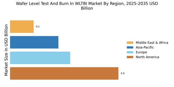
    The regional market segmentation of the Wafer Level Test And Burn In Wltbi Market exhibits diverse growth patterns across different regions. North America is projected to maintain its dominance in the market, accounting for a significant share of the revenue in 2024 and beyond. The region's established semiconductor industry, coupled with the presence of major players, drives market growth.

    Europe follows North America in terms of market size, driven by increasing demand for advanced wafer-level testing and burn-in solutions in various industries.The APAC region is expected to witness substantial growth over the forecast period, owing to the rising adoption of electronics and the expansion of the semiconductor industry in countries like China, South Korea, and Taiwan. South America and MEA hold relatively smaller market shares, but they present opportunities for growth as the adoption of advanced technologies gains momentum.

    Regional variations in market size, growth rates, and competitive dynamics influence the overall market landscape of the Wafer Level Test And Burn In Wltbi Market. 

    Wafer Level Test And Burn In Wltbi Market Regional

    Source: Primary Research, Secondary Research, Market Research Future Database and Analyst Review

    Key Players and Competitive Insights

    Major players in the Wafer Level Test And Burn In Wltbi Market industry are focusing on expanding their presence and product portfolio to cater to the increasing demand for advanced testing and burn-in services. Leading Wafer Level Test And Burn In Wltbi Market players are investing heavily in research and development to offer innovative solutions and meet the evolving needs of the electronics industry.

    The Wafer Level Test And Burn In Wltbi Market development is being driven by the growing demand for high-quality and reliable electronic devices, the increasing adoption of advanced packaging technologies, and the need for efficient and cost-effective testing and burn-in processes. The competitive landscape of the Wafer Level Test And Burn In Wltbi Market is characterized by the presence of established players as well as emerging companies offering specialized solutions.ASE Technology is a leading provider of wafer-level testing and burn-in services to the semiconductor industry.

    The company has a strong presence in the Asia-Pacific region and offers a range of testing and burn-in solutions for a variety of semiconductor devices, including integrated circuits (ICs), system-on-chips (SoCs), and memory devices. ASE Technology is committed to providing high-quality testing and burn-in services to its customers and has invested heavily in advanced testing equipment and technologies.Xilinx is a leading provider of programmable logic devices (PLDs) and field-programmable gate arrays (FPGAs). The company offers a range of testing and burn-in services for its PLDs and FPGAs, including wafer-level testing, package-level testing, and system-level testing.

    Xilinx is committed to providing high-quality testing and burn-in services to its customers and has invested heavily in advanced testing equipment and technologies.

    Key Companies in the Wafer Level Test Burn In Market market include

    Industry Developments

    The Wafer Level Test And Burn In WLTBI market is projected to reach USD 4.08 billion by 2032, exhibiting a CAGR of 10.38% during the forecast period (2024-2032). The market growth is attributed to the rising demand for advanced packaging technologies, increasing adoption of wafer-level testing in semiconductor manufacturing, and growing demand for high-performance computing and artificial intelligence applications. Recent developments in the market include the introduction of new test systems with enhanced capabilities, such as higher throughput and improved accuracy. Additionally, collaborations between industry players to develop innovative solutions are expected to drive market growth in the coming years.

    .webp

    Future Outlook

    Wafer Level Test Burn In Market Future Outlook

    The Wafer Level Test and Burn In (WLTBI) Market is projected to grow at a 10.38% CAGR from 2024 to 2035, driven by technological advancements and increasing demand for miniaturized electronics.

    New opportunities lie in:

    • Development of advanced automated testing solutions for enhanced efficiency.
    • Expansion into emerging markets with tailored WLTBI services.
    • Integration of AI-driven analytics for predictive maintenance and quality assurance.

    By 2035, the WLTBI market is expected to achieve substantial growth, reflecting its critical role in semiconductor manufacturing.

    Market Segmentation

    Wafer Level Test Burn In Market Test Type Outlook

    • Functional Test
    • Parametric Test
    • Reliability Test

    Wafer Level Test Burn In Market Technology Outlook

    • Electrical Test (e-test)
    • Burn-In Test
    • Optical Inspection

    Wafer Level Test Burn In Market Application Outlook

    • Semiconductors
    • Integrated Circuits (ICs)
    • Microprocessors
    • Memory Devices

    Wafer Level Test Burn In Market Form Factor Outlook

    • Wafer-Level
    • Package-Level
    • Die-Level

    Wafer Level Test Burn In Market End-Use Industry Outlook

    • Automotive
    • Consumer Electronics
    • Industrial
    • Aerospace Defense

    Report Scope

    MARKET SIZE 20242.044(USD Billion)
    MARKET SIZE 20252.257(USD Billion)
    MARKET SIZE 20356.059(USD Billion)
    COMPOUND ANNUAL GROWTH RATE (CAGR)10.38% (2024 - 2035)
    REPORT COVERAGERevenue Forecast, Competitive Landscape, Growth Factors, and Trends
    BASE YEAR2024
    Market Forecast Period2025 - 2035
    Historical Data2019 - 2024
    Market Forecast UnitsUSD Billion
    Key Companies ProfiledMarket analysis in progress
    Segments CoveredMarket segmentation analysis in progress
    Key Market OpportunitiesAdvancements in semiconductor technology drive demand for efficient Wafer Level Test And Burn In WLTBI solutions.
    Key Market DynamicsTechnological advancements drive efficiency in Wafer Level Test and Burn In processes, enhancing semiconductor performance and reliability.
    Countries CoveredNorth America, Europe, APAC, South America, MEA

    Leave a Comment

    FAQs

    What is the current market size of the Wafer Level Test And Burn In Wltbi Market?

    Wafer Level Test Burn In Market is expected to grow with a CAGR of 10.38% in the period 2025-2035

    Which region holds the largest share in the Wafer Level Test And Burn In Wltbi Market?

    North America currently holds the largest share in the Wafer Level Test And Burn In Wltbi Market, owing to the presence of major semiconductor manufacturers and a well-established electronics industry in the region.

    What are the key factors driving the growth of the Wafer Level Test And Burn In Wltbi Market?

    The growth of the Wafer Level Test And Burn In Wltbi Market is primarily attributed to the increasing demand for high-performance semiconductors, the adoption of advanced packaging technologies, and the growing adoption of artificial intelligence (AI) and machine learning (ML) applications.

    Who are the key competitors in the Wafer Level Test And Burn In Wltbi Market?

    Some of the key competitors in the Wafer Level Test And Burn In Wltbi Market include Teradyne, Inc., Advantest Corporation, Cohu, Inc., and FormFactor, Inc.

    What are the major applications of Wafer Level Test And Burn In Wltbi solutions?

    Wafer Level Test And Burn In Wltbi solutions are primarily used in the testing and burn-in of semiconductor wafers, which are essential components in various electronic devices such as smartphones, laptops, and servers.

    What is the expected growth rate of the Wafer Level Test And Burn In Wltbi Market in the coming years?

    Wafer Level Test Burn In Market is projected to grow at a CAGR of 10.38% during the forecast period, 2025-2035

    Which industry verticals are expected to contribute significantly to the growth of the Wafer Level Test And Burn In Wltbi Market?

    The automotive, consumer electronics, and data center industries are anticipated to be major contributors to the growth of the Wafer Level Test And Burn In Wltbi Market, driven by the increasing adoption of advanced technologies in these sectors.

    What are the emerging trends shaping the Wafer Level Test And Burn In Wltbi Market?

    Emerging trends in the Wafer Level Test And Burn In Wltbi Market include the adoption of 3D wafer-level packaging, the integration of AI and ML algorithms for data analysis, and the growing emphasis on sustainable and energy-efficient solutions.

    What challenges are faced by the Wafer Level Test And Burn In Wltbi Market?

    The Wafer Level Test And Burn In Wltbi Market faces challenges such as the high cost of equipment and materials, the need for skilled labor, and the rapid technological advancements that can lead to market volatility.

    What opportunities exist for growth in the Wafer Level Test And Burn In Wltbi Market?

    Opportunities for growth in the Wafer Level Test And Burn In Wltbi Market include the expansion of semiconductor manufacturing facilities, the increasing adoption of AI and ML in device testing, and the growing demand for high-performance computing applications.

    Download Free Sample

    Kindly complete the form below to receive a free sample of this Report

    Case Study
    Chemicals and Materials

    Compare Licence

    ×
    Features License Type
    Single User Multiuser License Enterprise User
    Price $4,950 $ $7,250
    Maximum User Access Limit 1 User Upto 10 Users Unrestricted Access Throughout the Organization
    Free Customization
    Direct Access to Analyst
    Deliverable Format
    Platform Access
    Discount on Next Purchase 10% 15% 15%
    Printable Versions