• Cat-intel
  • MedIntelliX
  • Resources
  • About Us
  • Request Free Sample ×

    Kindly complete the form below to receive a free sample of this Report

    Leading companies partner with us for data-driven Insights

    clients tt-cursor

    US Wafer Inspection System Market

    ID: MRFR/SEM/15774-HCR
    200 Pages
    Garvit Vyas
    September 2025

    US Wafer Inspection System Market Research Report By Technology (E-Beam Detection Technology, Optical Detection Technology) and By Defect Type (Random Defects Detection, Systematic Defects Detection) - Forecast to 2035

    Share:
    Download PDF ×

    We do not share your information with anyone. However, we may send you emails based on your report interest from time to time. You may contact us at any time to opt-out.

    US Wafer Inspection System Market Research Report -Forecast till 2035 Infographic
    Purchase Options
    $ 4,950.0
    $ 5,950.0
    $ 7,250.0

    US Wafer Inspection System Market Summary

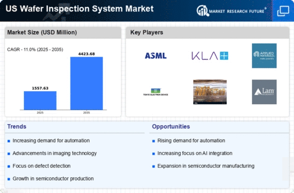
    The United States Wafer Inspection System market is projected to grow significantly from 1.5 USD billion in 2024 to 4 USD billion by 2035.

    Key Market Trends & Highlights

    US Wafer Inspection System Key Trends and Highlights

    • The market is expected to experience a compound annual growth rate of 9.33 percent from 2025 to 2035.
    • By 2035, the market valuation is anticipated to reach 4 USD billion, indicating robust growth opportunities.
    • In 2024, the market is valued at 1.5 USD billion, reflecting the current demand for advanced wafer inspection technologies.
    • Growing adoption of automation in semiconductor manufacturing due to increasing production efficiency is a major market driver.

    Market Size & Forecast

    2024 Market Size 1.5 (USD Billion)
    2035 Market Size 4 (USD Billion)
    CAGR (2025-2035) 9.33%

    Major Players

    Tokyo Electron, ASML Holding, Lam Research Corporation, KLA Corporation, Nikon Corporation, Screen Holdings, CyberOptics, Cohu, Advantest Corporation, Veeco Instruments, Rudolph Technologies, Hitachi HighTechnologies, Qorvo, Teradyne, Applied Materials

    US Wafer Inspection System Market Trends

    In the US Wafer Inspection System Market, there is a noticeable trend towards increasing automation and digitalization in semiconductor manufacturing. This shift is driven by the need for higher precision and efficiency in the production process. As manufacturers seek to enhance yields and maintain quality, advanced inspection systems utilizing AI and machine learning are gaining traction. Companies are investing in these technologies to automate defect detection and reduce the time and costs associated with manual inspections. Another key driver for the market is the upsurge in demand for semiconductors across various industries, including automotive, consumer electronics, and telecommunications.

    The growth in these sectors is putting pressure on manufacturers to improve production capabilities, thereby creating opportunities for innovative wafer inspection solutions. The recent focus on sustainability and eco-friendly practices is also influencing the US market. Companies are exploring wafer inspection technologies that minimize waste and reduce energy consumption, aligning their operations with environmental standards. This presents opportunities for manufacturers who can develop systems that meet these needs while delivering high-performance outcomes. 

    In terms of trends, there is a growing emphasis on in-line inspection techniques which allow for real-time monitoring of the wafer production process.This approach enables manufacturers to identify and address defects immediately, reducing the likelihood of costly recalls and reprocessing. With the ongoing developments in technology and manufacturing processes, the US Wafer Inspection System Market is poised for significant evolution, reflecting the changing landscape of the semiconductor industry and meeting the increasing demands for advanced manufacturing solutions.

    Market Segment Insights

    Wafer Inspection System Market Technology Insights

    The US Wafer Inspection System Market is witnessing significant advancements within the Technology segment, focusing primarily on innovations in E-Beam Detection Technology and Optical Detection Technology. The increasing demand for accurate and high-resolution inspection systems aligns with the growing complexity of semiconductor manufacturing processes. E-Beam Detection Technology is increasingly recognized for its ability to identify defects at a nanometer scale, which is critical for the production of advanced microelectronics. This technology provides a superior resolution compared to traditional methods, making it an essential component in maintaining quality standards in wafer fabrication. 

    On the other hand, Optical Detection Technology continues to be a vital component of the market, leveraging light-based methods for defect inspection. This technology is widely adopted due to its speed and efficiency, making it suitable for high-volume production environments. The capability to quickly detect defects without causing damage to wafers makes Optical Detection Technology particularly beneficial in processing delicate substrates.

    The integration of sophisticated algorithms and artificial intelligence in both detection technologies further enhances their effectiveness, allowing for real-time analysis and improved throughput in manufacturing environments.The growth in these technologies is driven by the relentless pursuit of miniaturization in electronic components and the increasing need for higher yields in semiconductor production. 

    Additionally, the push for more resilient and energy-efficient devices is propelling advancements in wafer inspection technologies. As the US Wafer Inspection System Market continues to evolve, businesses are increasingly investing in both E-Beam and Optical Detection Technologies. These technologies not only help in enhancing the quality of semiconductor products but also play a significant role in reducing operational costs related to defect detection and management. The ongoing innovations in these areas highlight the importance of continuous Research and Development efforts in maintaining a competitive edge within the US Wafer Inspection System Market.

    Overall, the future of the Technology segment looks promising, given its critical role in ensuring the reliability and performance of semiconductor devices across various applications.

    Wafer Inspection System Market Defect Type Insights

    The US Wafer Inspection System Market is significantly influenced by the Defect Type segment, which serves as a critical factor in maintaining the quality and reliability of semiconductor manufacturing. This segment is primarily divided into Random Defects Detection and Systematic Defects Detection, each catering to different aspects of defect management. Random Defects Detection focuses on identifying sporadic issues that can arise during the wafer fabrication process, playing a crucial role in ensuring product uniformity and reliability in high-volume production.

    On the other hand, Systematic Defects Detection addresses consistent, recurring issues tied to specific tools or processes, thereby enhancing the manufacturing workflow and minimizing the risk of yield loss. The rising complexity of semiconductor devices, driven by innovations in technology and the increasing demand for high-performance integrated circuits, propels the need for adept detection methods. As such, both detection types are poised to remain vital for the industry's growth, bolstering efficiency and product quality standards in the competitive US market.The advancements in inspection technologies and methodologies are crucial as manufacturers strive to meet stringent performance targets and reduce operational costs.

    Get more detailed insights about US Wafer Inspection System Market Research Report -Forecast till 2035

    Key Players and Competitive Insights

    The competitive landscape of the US Wafer Inspection System Market is characterized by various factors, including technological advancements, market demand, and the presence of key players who drive innovation and quality. As semiconductor manufacturing continues to evolve, the need for advanced inspection systems becomes increasingly critical in ensuring the production of high-quality wafers. Companies participating in this market are engaged in constant research and development efforts to enhance their offerings, further strengthening their positions. 

    The market is underscored by a diverse range of inspection technologies that cater to different stages of the semiconductor manufacturing process, thereby making competition intense as firms strive to meet the specific demands of manufacturers. With the integration of artificial intelligence and machine learning, inspection systems are becoming more efficient, prompting companies to strategically align their products with emerging technological trends while maintaining a keen eye on cost-control measures. In the US Wafer Inspection System Market, Tokyo Electron has established itself as a formidable player. The company’s strengths lie in its extensive experience and deep-rooted expertise in semiconductor manufacturing equipment.

    Tokyo Electron has developed a strong brand reputation built on reliability and performance, which resonates with customers looking for precision and efficiency in their manufacturing processes. 

    The company's focus on innovation is evident through its ongoing investments in research and development, aimed at enhancing the capabilities of its wafer inspection systems. Moreover, Tokyo Electron has a robust service network across the United States, allowing it to provide comprehensive support and maintenance solutions, which further solidifies its market presence. This commitment to customer service, along with the effective scalability of its products, positions Tokyo Electron favorably within the competitive matrix of the US market.ASML Holding has made significant strides within the US Wafer Inspection System Market, particularly with its flagship products that are pivotal in advanced photolithography. 

    Known for its cutting-edge Extreme Ultraviolet (EUV) lithography systems, ASML also offers comprehensive inspection tools that are integral in the wafer manufacturing process. The company has cultivated a strong foothold in the US market through strategic partnerships and collaborations with leading semiconductor manufacturers. ASML’s strengths include its innovative technology and a commitment to maintaining high standards of precision in semiconductor production. 

    The company has continuously focused on mergers and acquisitions to bolster its technological capabilities and extend its market reach. By integrating complementary technologies and enhancing production efficiencies through these strategic moves, ASML has reinforced its competitive positioning in the US Wafer Inspection System Market, ensuring that it remains at the forefront of the industry’s evolution.

    Key Companies in the US Wafer Inspection System Market market include

    Industry Developments

    Recent developments in the US Wafer Inspection System Market have shown significant growth and technological advancements. Notable companies such as Tokyo Electron, ASML Holding, and KLA Corporation continue to innovate, focusing on enhancing defect detection and process efficiency. For instance, in February 2023, Lam Research Corporation launched a new Advanced Patterning technology that revolutionizes wafer inspection processes. The market has also been influenced by increasing demand for semiconductors, with a reported growth rate of approximately 10% in the sector over the last year. 

    Regarding mergers and acquisitions, in March 2023, CyberOptics announced its acquisition of a technology firm specializing in sensor solutions, which enhances its position in the market. Additionally, in July 2022, Teradyne entered a strategic partnership with a prominent semiconductor manufacturer to improve inspection capabilities. Other major players like Veeco Instruments and Applied Materials are also expanding their market presence by investing in Research and Development to drive innovation. Overall, the US wafer inspection sector is witnessing accelerating growth fueled by technological advancements and strategic partnerships among leading firms.

    Market Segmentation

    Outlook

    • E-Beam Detection Technology
    • Optical Detection Technology

    Wafer Inspection System Market Technology Outlook

    • E-Beam Detection Technology
    • Optical Detection Technology

    Wafer Inspection System Market Defect Type Outlook

    • Random Defects Detection
    • Systematic Defects Detection

    Report Scope

    Report Attribute/Metric Source: Details
    MARKET SIZE 2018 1.12 (USD Billion)
    MARKET SIZE 2024 1.5 (USD Billion)
    MARKET SIZE 2035 4.0 (USD Billion)
    COMPOUND ANNUAL GROWTH RATE (CAGR) 9.326% (2025 - 2035)
    REPORT COVERAGE Revenue Forecast, Competitive Landscape, Growth Factors, and Trends
    BASE YEAR 2024
    MARKET FORECAST PERIOD 2025 - 2035
    HISTORICAL DATA 2019 - 2024
    MARKET FORECAST UNITS USD Billion
    KEY COMPANIES PROFILED Tokyo Electron, ASML Holding, Lam Research Corporation, KLA Corporation, Nikon Corporation, Screen Holdings, CyberOptics, Cohu, Advantest Corporation, Veeco Instruments, Rudolph Technologies, Hitachi HighTechnologies, Qorvo, Teradyne, Applied Materials
    SEGMENTS COVERED Technology, Defect Type
    KEY MARKET OPPORTUNITIES Rising demand for semiconductors, Advanced automation technologies implementation, Increasing investment in R&D, Growing adoption of AI integration, Shift towards more efficient processes
    KEY MARKET DYNAMICS Technological advancements, Increasing semiconductor demand, Growing automation trends, Rising investment in R&D, Competitive landscape intensification
    COUNTRIES COVERED US

    FAQs

    What is the expected market size of the US Wafer Inspection System Market in 2024?

    The US Wafer Inspection System Market is expected to be valued at 1.5 billion USD in 2024.

    What is the projected market size by 2035 for the US Wafer Inspection System Market?

    By 2035, the market size of the US Wafer Inspection System Market is anticipated to reach 4.0 billion USD.

    What is the expected compound annual growth rate (CAGR) for the US Wafer Inspection System Market from 2025 to 2035?

    The expected CAGR for the US Wafer Inspection System Market from 2025 to 2035 is 9.326%.

    Which technology segment is expected to dominate the US Wafer Inspection System Market in 2024?

    The Optical Detection Technology segment is expected to dominate the market with a valuation of 0.9 billion USD in 2024.

    What will be the market value for E-Beam Detection Technology by 2035?

    E-Beam Detection Technology is projected to reach a market value of 1.5 billion USD by 2035.

    What are the key players in the US Wafer Inspection System Market?

    Major players in the market include Tokyo Electron, ASML Holding, KLA Corporation, and Lam Research Corporation.

    What is the expected growth rate for the Optical Detection Technology segment between 2025 to 2035?

    The Optical Detection Technology segment is projected to grow to 2.5 billion USD by 2035.

    What impact will the current global scenario have on the US Wafer Inspection System Market?

    The current global scenario may influence supply chains and demand dynamics, impacting market growth.

    What challenges does the US Wafer Inspection System Market face moving forward?

    The market faces challenges such as rapid technological advancements and supply chain uncertainties.

    Which regions are expected to contribute significantly to the growth of the US Wafer Inspection System Market?

    The North American region, specifically the United States, is expected to be a significant contributor to market growth.

    Report Infographic
    Free Sample Request

    Kindly complete the form below to receive a free sample of this Report

    Customer Strories

    “I am very pleased with how market segments have been defined in a relevant way for my purposes (such as "Portable Freezers & refrigerators" and "last-mile"). In general the report is well structured. Thanks very much for your efforts.”

    Victoria Milne Founder
    Case Study

    Chemicals and Materials