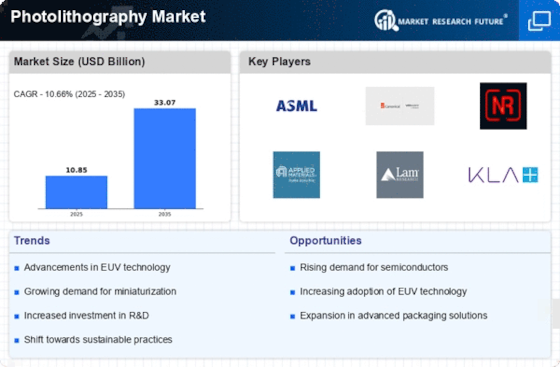
Miniaturization is a major trend. As demand for smaller and more powerful electronics rises, semiconductor makers are perfecting photolithography procedures to attain finer resolutions. Advanced lithography equipment that can produce detailed patterns on semiconductor wafers is needed to make innovative microchips.
Rising extreme ultraviolet lithography is another trend. Photolithography has advanced to EUV lithography, which uses shorter wavelength light to make chip details. As semiconductor makers seek solutions to overcome optical lithography's constraints, this trend is growing. EUV lithography is becoming commonplace, improving precision and enabling high-performance semiconductor devices.
Photolithography is also influenced by automation and Industry 4.0. Automation, artificial intelligence, and data analytics are improving photolithography output, efficiency, and accuracy. Real-time photolithography equipment monitoring and control are becoming common in smart manufacturing, improving yield and operational excellence.
In photolithography, sustainability is becoming more important. Industry participants are adopting eco-friendly production strategies as environmental awareness rises. More energy-efficient, chemical-efficient, and recyclable equipment is being developed. Sustainable practices support global environmental goals and appeal to consumers and businesses seeking green solutions.
Advanced semiconductor devices are in demand due to IoT and 5G technologies, influencing photolithography market trends. These technologies require high-performance, energy-efficient devices, therefore semiconductor makers buy cutting-edge lithography equipment. As connected devices proliferate and 5G networks are deployed, sophisticated semiconductor solutions are in demand, driving the photolithography market. Photolithography market consolidation is another trend.
Finally, photolithography solutions are becoming more tailored and application-specific. Customized photolithography procedures are needed as more businesses use semiconductor technology. Companies are reacting by developing flexible and adaptable solutions for car electronics and medical equipment."
Photolithography Market Size was valued at USD 9.65 Billion in 2023. The Photolithography market industry is projected to grow from USD 10.85 Billion in 2024 to USD 24.42 Billion by 2032, exhibiting a compound annual growth rate (CAGR) of 10.66% during the forecast period (2024 - 2032). The key market drivers contributing to market growth and expansion are the electronics industry growth, increased computer chip manufacturing, and increased need for photolithography and improvements in Photolithography processes.
Source: Secondary Research, Primary Research, MRFR Database, and Analyst Review
The rising electronics industry is driving the market CAGR for Photolithography. The key forces driving the industry's expansion are the worldwide growth of the end-user electronics sector and the arrival of advanced electronics items by global market participants. As indicated by industry analysts, rising requirements for photolithography in the fabrication of boards for printed circuits and processors, a rise in the manufacturing of computing chips, a boost in the requirement for photolithography in the IC (integrated circuit) sector, and a rapidly expanding global electronics packaging market will all be contributing to the market's development during the forecast period. Photolithography technology offers several advantages, including high light sensitivity, outstanding adhesion properties, high resolution, and the capacity to 3D encapsulate cells within hydrogels, propelling the industry forward.
Additionally, photolithography process advancements are expected to give profitable chances for market expansion on a global scale. Furthermore, the trend of manufacturers towards downsizing to increase the usage of handheld devices has created a slew of opportunities in the Photolithography Market. But the inherent complexity of the manufacturing process, in addition to the constant evolution of the semiconductor industry, may serve as a future impediment to the growth of the global photolithography approach.
According to industry experts, the coronavirus outbreak's worldwide impact is expected to significantly impact the growth of the photolithography consumer market in 2020. According to government officials, travel restrictions, a halt to overseas activities, and the closure of companies and manufacturing facilities have all been implemented due to the pandemic. Over forty countries have declared a state of emergency, resulting in stock market returns, severe delays in logistical processes, and an uncertain future. According to MRF research, the photolithography industry is predicted to pick up steam by the second half of 2021 after achieving a median expansion rate in the first quarter of the previous year. This product's demand is most likely from the deep ultraviolet (DUV) industry. According to current projections, the pandemic will cause a contraction in economic activity over the next two or three quarters, leading the economy to decline. Businesses are expected to resume operations as the closure restrictions are eased individually gradually. For instance, by the Department of Electronics and Information Technology, around 2,000 chips are created in India each year, with over 20,000 engineers working on chip design and verification. Thus, it is anticipated that demand for photolithography will increase throughout the projected timeframe due to the rising electronics industry. Thus, driving the Photolithography market revenue.
The Photolithography Market segmentation, based on Process, includes Deep Ultraviolet [DUV], Extreme Ultraviolet [EUV], I-line, Krypton Fluoride [KrF], Argon Fluoride [ArF] Dry. The extreme ultraviolet [EUV] segment dominated the market, accounting for 38% of market revenue (USD 3.3 Billion) in 2022. As the semiconductor sector expanded, so did the demand for intense UV procedures for producing electronic components. To manufacture semiconductor devices, manufacturing companies ought to place expensive wafers on each wafer. Consequently, companies benefit from the EUV process since it exposes the critical level in just one phase, cutting the cost of producing semiconductor devices. The EUV technology uses a laser-created plasma lighting source, which reduces repair and operational expenses. As an outcome, producers are concentrating on extreme UV photolithography, propelling the sector ahead. Furthermore, microprocessors developed by EUV are strong, smart, and extremely efficient.
The Photolithography Market segmentation, based on Applications, includes Front-End and Back-End. The back-end category generated the highest market revenue of about 52% (USD 4.5 billion) 2022. The back-end process includes wafer backgrounding, mounting, cutting, die-attach cure, labeling, lead finishing, post-mold cure, molding, wire connection, trim, the ultimate test, final visual inspection, packaging, and shipment. Because of innovations and breakthroughs in the semiconductor sector's front-end process, the development pace for back-end photolithography has decreased. Nonetheless, the introduction of MLE equipment is advantageous for back-end photolithography.
Figure 1: Photolithography Market, by Application, 2022 & 2032 (USD Billion)
Source: Secondary Research, Primary Research, MRFR Database, and Analyst Review
By region, the research provides market insights into North America, Europe, Asia-Pacific, and the Rest of the World. The North American Photolithography market area will dominate during the projected timeframe because of technical advances, inventions, and industrial investments, boosting the market growth in the North American region.
Furthermore, the major countries studied in the market report are the US, Canada, German, France, the UK, Italy, Spain, China, Japan, India, Australia, South Korea, and Brazil.
Figure 2: Photolithography Market Share by Region 2022 (USD Billion)
Source: Secondary Research, Primary Research, MRFR Database, and Analyst Review
Europe region’s Photolithography market accounts for the second-highest market share due to a rise in the usage of electrical power modules. It uses, as well as several electronic apps. Further, the German Photolithography market holds the largest market share, and the UK Photolithography market is expected to grow and expand significantly in the European region during the projected timeframe.
The Asia-Pacific Photolithography Market is expected to grow quickly during the projected timeframe. This is due to the growing need for high-voltage working devices, which will boost the overall market growth. Moreover, China’s Photolithography market dominates the market share, and the Indian Photolithography market is expected to expand and grow steadily in the Asia-Pacific region during the projected timeframe.
Leading market players invested heavily in research and Development (R&D) to scale up their manufacturing units and develop technologically advanced solutions, which will help the Photolithography market grow worldwide. Market participants are also undertaking various organic or inorganic strategic approaches to strengthen and expand their global footprint, with significant market developments including new product portfolios, contractual deals, mergers and acquisitions, capital expenditure, higher investments, and strategic alliances with other organizations. Businesses are also coming up with marketing strategies such as digital marketing, social media influencing, and content marketing to increase their scope of profit earnings. The Photolithography industry must offer cost-effective and sustainable options to survive in a highly fragmented and dynamic market climate.
Manufacturing locally to minimize operational expenses and offer aftermarket services to customers is one of the critical business strategies organizations use in the global Photolithography industry to benefit customers and capture untapped market share and revenue. The Photolithography industry has recently offered the Silicon, Wafer, and Fabrication industry significant advantages. Moreover, more industry participants are utilizing and adopting cutting-edge Technology has grown substantially. Major players in the Photolithography market, including General Mills Inc., Amway, Conagra Brands Inc., Cargill Incorporated, Abbott Laboratories, Kraft Foods Group Inc., and others, are attempting to expand market share and demand by investing in R&D operations to produce sustainable and affordable solutions.
Nikon firm, often known simply as Nikon, is a Japanese multinational firm headquartered in Tokyo that specializes in developing and marketing optical and image technologies. The Nikon Group is made up of the companies that Nikon owns. Nikon offers goods and services centered around Opto-Electronics Sciences and Precision Systems, as well as its company concept of Credibility and Creativity. A multinational corporation contributes to realizing a more affluent society by reacting to people's and industries' wishes and aspirations. Nikon Corporation unveiled the Lasermeister 100A, an optical processor machine that uses a laser to treat different metals, in April 2019. It is capable of laser labeling, the welding process, and 3D printing. These systems use superior optical and precise control technology to construct that yield high-quality outputs.
Canon, Inc. develops, manufactures, and sells office multifunction devices, copiers, printing devices, photographic equipment, and lithography equipment. It is divided into four business units: Professional Business Unit (BU), Imaging Network BU, Healthcare System BU, and Industrial and Others BU. The corporation was established on August 10, 1937, and is based in Tokyo, Japan. Canon Inc. released its initial semiconductor lithography machinery, the FPA-8000iW, in July 2020, allowing the manufacture of semiconductor devices utilizing huge panels widely utilized in back-end computing.
Samsung Electronics (South Korea)
Carl Zeiss AG (Germany)
ASML Holding NV (Netherlands)
Applied Materials Inc. (US)
Taiwan Semiconductor Manufacturing Company Limited (Taiwan)
JEOL Ltd (Japan)
Rudolph Technologies Inc. (US)
NIL TECHNOLOGY (Denmark)
Shanghai Micro Electronics Equipment (Group) Co. Ltd
EV Group (EVG) (Austria)
July 2020: Canon Inc. released its initial semiconductor lithography machinery, the FPA-8000iW, in July 2020, allowing the manufacture of semiconductor devices utilizing huge panels widely utilized in back-end computing.
August 2019: SCHOTT & EV Corporation partnered in August 2019 to demonstrate the preparedness of 12-inch nanoimprint lithography technology for large quantities of structuring of high-refractive-index glass wafers utilized for fabricating wavelength and optical guides for augment and virtual reality headsets.
April 2019: Nikon Corporation unveiled the Lasermeister 100A, an optical processor machine that uses a laser to treat different metals, in April 2019. It is capable of laser labeling, the welding process, and 3D printing. These systems use superior optical and precise control technology to construct that yield high-quality outputs.
Deep Ultraviolet [DUV]
Extreme Ultraviolet [EUV]
I-line
Krypton Fluoride [KrF]
Argon Fluoride [ArF] Dry
Front-End
Back-End
North America
US
Canada
Europe
Germany
France
UK
Italy
Spain
Rest of Europe
Asia-Pacific
China
Japan
India
Australia
South Korea
Australia
Rest of Asia-Pacific
Rest of the World
Middle East
Africa
Latin America
© 2024 Market Research Future ® (Part of WantStats Reasearch And Media Pvt. Ltd.)