Automated test equipment is witnessing a few remarkable trends with inflation driving the market for automation through its unforgivable form in which it fervently leaves Innovations to discuss innovation. The packaging, for instance, of chips or semiconductor devices is a significant component in the protection and interconnection aspects. The current trends are an indication of dynamic change seen across the marketplace sounding the alarm bells l with ripples that shake circle upon circle. A major trend is the increasing sophistication and added complexities in response to vast changing performance needs of devices. With the way semiconductor manufacturers continue to pursue ways of improving what a chip is capable of yielding, the market is migrating towards new technologies that include 3D packaging, wafer-level packaging, and fan-out level processing. These advanced packaging methods provide the performance, power efficiency in addition to form factor within the desires of various applications through electronics telecommunication along with automotive industries.
Increasing AI and IoT trends incorporate strongly with Chip Packaging Market Of significant interest. Semiconductors that can deliver increased processing power and improved efficiency have found multiple applications in the digital world possibly due to widespread deployment of AI and IoT technologies used in smart devices, autonomous vehicles, futuristic edge computing infrastructure etc. This need is guiding the market towards chip packaging alternatives that can support higher data transport speeds, decreased power expenditure, and better thermals. However, the cutting-edge technologies in packaging such as heterogeneous integration are gaining momentum to meet unique demands of the AI and IoT market. Miniaturization and size reduction never cease to be a trait peculiar for the semiconductor industry; moreover, the Chip Packaging market flaunts such traits just alike. While the demands for larger, more spacious packaging appear to be insatiable in some industries, smaller and compact packaging solutions are also important due to the portable nature of electronic devices and wearables especially. Chip-scale packaging (CSP) and system in package technologies (SiP), are taking the industry by storm, as these two emerging solutions allow for multiple functions or components to be integrated into a single, compact package. This tendency does justice to proliferation of consumer’s electronics which seek for smaller and more powerful devices.
The sustainability issues are growing in prominence, as evident from the Chip Packaging market. The issue of environmental impact is a critical one for the electronics industry today. As pressure is placed on manufacturers to focus upon reductions in waste and reduce energy use, pallets as a form pf packaging also represent an important area of development where material reduction or unused space could help improve efficiency levels across logistic chains. The market is seeing evolvement in the packaging career that consists of environmentally friendly materials and processes with essence on recyclability smart erode fewer carbon foot-prints. Innovations in the area of eco-friendly chip packaging solutions are expected to make headways as semiconductors and electronics companies look for sustainable packaging options that would synergize their activities with global environmental initiatives.
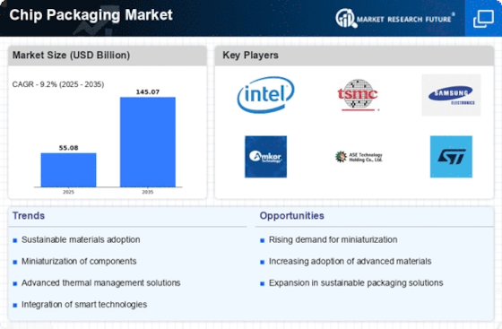
The Chip Packaging market industry is projected to grow from USD 76.2 billion by 2032, exhibiting a compound annual growth rate (CAGR) of 9.20% during the forecast period (2024 - 2032). Increased demand for miniaturization and performance optimization of electronic devices and demand for advanced packaging solutions are the key market drivers enhancing growth of the market.
Source: The Secondary Research, Primary Research, MRFR Database and Analyst Review
Market CAGR for chip packaging is being driven by the rising demand for miniaturization and performance optimization of electronic devices. As consumer expectations for compact and lightweight electronic devices rise, there is a growing need for chip packaging solutions that enable the creation of smaller form factors. Advanced packaging technologies allow semiconductor components to be densely packed, contributing to the miniaturization of electronic devices such as smartphones, wearables, and IoT devices.
Miniaturized electronic devices often face challenges related to heat dissipation. Advanced chip packaging techniques include features such as integrated heat sinks, thermal vias, and advanced materials that help manage and dissipate heat efficiently. This is crucial for maintaining the performance and reliability of high-powered electronic components. The demand for performance optimization in electronic devices goes hand in hand with the need for enhanced electrical performance. Advanced chip packaging allows for the integration of multiple functionalities into a single package, minimizing signal delays and optimizing the overall electrical performance of semiconductor devices. Modern electronic devices often require the integration of diverse semiconductor components, such as processors, memory, sensors, and communication modules. Advanced chip packaging technologies facilitate the integration of these heterogeneous components in a compact and interconnected manner, enabling seamless communication and improving overall device performance.
Miniaturization, coupled with advanced chip packaging, allows for the incorporation of higher levels of functionality within limited physical space. This is crucial for devices such as smartwatches, medical implants, and automotive electronics, where space constraints are significant, but the demand for diverse functionalities remains high. Miniaturization and optimized chip packaging contribute to energy efficiency in electronic devices. By reducing the distances that signals need to travel within a device, power consumption can be minimized. This is especially important for battery-powered devices where energy efficiency directly impacts the device's longevity between charges. Consumer preferences drive the demand for smaller, more powerful electronic devices. The market demand for compact consumer electronics, coupled with the need for improved performance, incentivizes semiconductor manufacturers to invest in advanced chip packaging technologies to stay competitive and meet consumer expectations.
The increasing demand for miniaturization and performance optimization in electronic devices is a key driver for the chip packaging market. Advanced packaging solutions enable semiconductor manufacturers to address the challenges posed by shrinking device sizes while meeting the ever-growing expectations for enhanced performance and functionality in modern electronics. Thus driving the Chip Packaging market revenue.
The Chip Packaging Market segmentation, based on type, includes Fan-Out Wafer-Level Packaging, Fan-In Wafer-Level Packaging, Flip Chip, and 2.5D/3D. The fan-out wafer-level packaging segment dominates the market, accounting for the largest market revenue due to its versatility, compact design, and ability to accommodate heterogeneous integration. FOWLP allows for the placement of multiple chips on a single substrate, enabling higher levels of integration in a smaller footprint. Its flexibility in supporting various chip sizes and types makes it well-suited for diverse applications, from consumer electronics to high-performance computing. Additionally, FOWLP's cost-effectiveness and efficiency in handling thermal management challenges contribute to its widespread adoption, positioning it as a dominant and preferred packaging type in the evolving semiconductor industry.
The Chip Packaging Market segmentation, based on application, includes Telecommunications, Automotive, Aerospace and Defense, Medical Devices, and Consumer Electronics. The consumer electronics category dominates the market due to the relentless pursuit of miniaturization, enhanced performance, and innovative features in devices such as smartphones, tablets, and wearables. The demand for smaller and powerful electronic gadgets necessitates advanced chip packaging technologies that enable the integration of complex semiconductor components within limited space. Additionally, consumer electronics manufacturers prioritize aesthetics and form factors, driving the adoption of chip packaging solutions that support sleek designs and compact dimensions. Further, telecommunication is the second-largest application for chip packaging due to the growing demand for high-speed and high-performance telecommunications networks.
Source: The Secondary Research, Primary Research, MRFR Database and Analyst Review
By region, the study gives market insights into the North America, Europe, Asia-Pacific, and the Rest of the World. The North American Chip Packaging market area will dominate this market due to its technological innovation ecosystem, a strong presence of leading semiconductor companies, and substantial investments in research and development. The region's leadership is further reinforced by its significant contribution to advanced applications.
Further, the prime countries studied in the market report are The US, Canada, Germany, France, the UK, Italy, Spain, Japan, China, India, Australia, South Korea, and Brazil.
Source: The Secondary Research, Primary Research, MRFR Database and Analyst Review
The Europe Chip Packaging Market is expected to rise at the fastest CAGR in the forecast period. The growing need for creative packaging solutions to support the semiconductor industry, along with the region's emphasis on R&D, industry player collaborations, and packaging technology advancements, are what are driving the demand for chip packaging. Additionally, the growing importance of energy efficiency and miniaturisation in electronic devices is also a contributing factor. Moreover, Germany Chip Packaging market held the largest market share, and the UK Chip Packaging market was the fastest-growing market in Asia-Pacific region.
The Asia-Pacific Chip Packaging Market is expected to rise at the fastest CAGR 9.20% from 2023 to 2032. This is due to the region's central role in electronics manufacturing, the growing demand for consumer electronics, and the increasing adoption of advanced semiconductor technologies across various industries. Moreover, China’s Chip Packaging market held the largest market share, and the Indian Chip Packaging market was the fastest-growing market in Asia-Pacific region.
Leading market players are investing heavily in the research and development in order to expand their product lines, which will help the Chip Packaging market grow even more. Market players are also undertaking a variety of strategic activities to spread their global footprint, with important market developments including mergers and acquisitions, new product launches, contractual agreements, higher investments, and collaboration with other organizations. To spread and survive in a more competitive and rising market climate, the Chip Packaging industry must offer cost-effective items.
Manufacturing locally to minimize the operational costs is one of the key business tactics used by the manufacturers in the global Chip Packaging industry to benefit the clients and increase the market sector. In recent years, the Chip Packaging industry has offered some of the most significant advantages to several industries. Major players in the Chip Packaging market, including Amkor Technology Inc., Intel Corporation, Samsung Electronics Co., Ltd., SK Hynix Inc., Qualcomm Incorporated, NXP Semiconductors NV, Texas Instruments Incorporated, Micron Technology Inc., Taiwan Semiconductor Manufacturing Company Ltd, Advanced Semiconductor Engineering, Inc., and others, are trying to increase market demand by investing in the research and development operations.
Amkor Technology is a globally recognized provider of semiconductor packaging and test services, playing a pivotal role in the semiconductor industry. Established in 1968 and headquartered in Tempe, Arizona, the company has evolved into one of the largest and most diverse semiconductor packaging and test service providers worldwide. Amkor specializes in providing advanced packaging solutions for integrated circuits, microprocessors, and other semiconductor devices, catering to a wider range of industries, including automotive, consumer electronics, and telecommunications. In August 2023, Amkor Technology and Advanced Semiconductor Engineering (ASE) announced a partnership to develop and offer advanced chip packaging solutions for next-generation semiconductor devices. The two companies compiled their strengths and expertise to develop new packaging technologies that meet the demanding requirements of high-performance applications such as artificial intelligence, machine learning, and 5G.
Advanced Semiconductor Engineering, Inc. (ASE) is a globally recognized provider of semiconductor manufacturing and testing services, with its headquarters in Kaohsiung, Taiwan. Established in 1984, ASE has become one of the leading companies in the semiconductor industry, offering a comprehensive range of services that include semiconductor packaging, assembly, testing, and design services. The company plays a critical role in the electronics supply chain, serving a diverse customer base that includes major semiconductor manufacturers, fabless companies, and integrated device manufacturers (IDMs). In April 2023, ASE announced a partnership with Nvidia to develop and offer advanced chip packaging solutions for Nvidia's data center and automotive graphics processing units (GPUs). The two companies will work together to develop new packaging technologies that enable Nvidia's GPUs to deliver even higher performance and power efficiency.
September 2023: Intel announced the acquisition of Tower Semiconductor, an Israeli semiconductor foundry, for $5.4 billion. This acquisition will give Intel access to Tower's specialty technology and chip packaging capabilities, which will help Intel meet the growing demand for advanced packaging solutions.
May 2023: Amkor Technology announced the acquisition of Xperi's wireless packaging business for $475 million. This acquisition will give Amkor access to Xperi's expertise in radio frequency (RF) and microwave packaging technologies, which are essential for developing next-generation wireless devices.
February 2023: Samsung Electronics announced that it will invest $17 billion to build a new chip packaging facility in Texas. This facility will help Samsung meet the growing demand for advanced packaging solutions in North America and expand its presence in the US semiconductor market.
© 2024 Market Research Future ® (Part of WantStats Reasearch And Media Pvt. Ltd.)