Market Analysis
Chip Packaging Market (Global, 2024)
Introduction
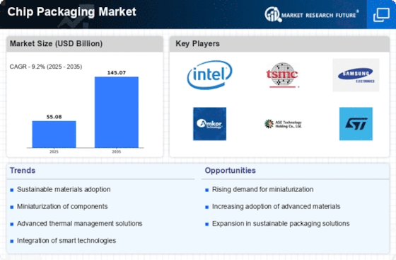
The chip-packaging industry is a vital component of the semiconductor industry, forming the crucial link between the integrated circuit and the outside world. As technology continues to advance, the need for ever-better chip packages, with their enhanced performance, miniaturization, and cost-efficiency, has risen sharply. The industry encompasses a wide range of products, from the relatively simple lead frame to the advanced flip-chip, and the newer three-dimensional packages, each of which can be used in a wide range of applications, from home appliances to automobiles and industrial equipment. The increasing complexity of semiconductors, together with the rising importance of green materials and energy conservation, is driving manufacturers to develop ever-more-evolved and efficient chip packages. In this context, a thorough understanding of the market is essential for anyone who wants to capitalize on the opportunities and seize the initiative.
PESTLE Analysis
- Political
- In 2024 the chip-package market was influenced by a number of political factors, including government policies designed to boost the domestic semiconductor industry. For example, the CHIPS Act allocated about fifty-two billion dollars to support research and development, and to stimulate the manufacturing of semiconductors. This had a direct effect on the chip-package industry by increasing the demand for advanced chip-packaging solutions. In addition, trade policies and tariffs imposed on semiconductors could affect supply chains. For example, the U.S. government imposed tariffs of up to twenty-five percent on certain imported components, which would raise the cost of production for companies that relied on foreign suppliers.
- Economic
- In 2024 the economic scene shows a strong demand for chip-packaging, caused by the growth of the electronics industry. The global market for electronics is expected to grow to $1,200 billion, of which a significant part will be attributed to the production of consumer, automobile and industrial applications. The average selling price of a chip-package is expected to be about 50 cents, which reflects the competitive situation. In this situation, the investment in new packaging technology is stimulated by the desire to increase performance and reduce costs.
- Social
- In 2024 the social trends are indicating an increased demand for sustainable and environmentally friendly products, which is influencing the chipboard packaging market. Around 70% of consumers are willing to pay a higher price for products with an environmental label, and this has led to a greater demand for sustainable materials and methods in the production of packaging. Also, the rise of smart devices and the IoT applications are increasing the demand for advanced packaging solutions that can meet the need for miniaturization and high performance, which corresponds to the consumers' need for high-tech devices.
- Technological
- In 2024, technological developments are transforming the chip-packaging market. The 3D-packaging technique is being increasingly used, with an estimated 30% of new products adopting this approach to increase performance and reduce space. Moreover, the integration of artificial intelligence into the design and manufacture of chip packages is expected to increase efficiency and reduce time to market. The R&D budgets of companies are increasing, with an estimated budget of fifteen billion dollars for chip-packaging innovations. The importance of technology in maintaining a competitive edge is becoming increasingly important.
- Legal
- Legal factors influencing the chip packaging market in 2024 are the stricter regulations on the environment and the intellectual property rights. In the European Union, the WEEE Directive, which regulates the disposal and recycling of electrical and electronic equipment, has had a major impact on the design and choice of materials for the packaging. The complex patent laws, in which more than 1,000 new patents on chip packaging were filed in 2024, have increased the importance of protecting innovations in chip packaging.
- Environmental
- In 2024, the market for chipboard packaging will be increasingly influenced by considerations of the environment, with a focus on reducing the carbon footprint and reducing waste. The chipboard industry accounts for about 2% of the world’s greenhouse gas emissions, and companies are therefore looking for ways to reduce their emissions. By 2030, many manufacturers want to reduce their emissions by 50%, which will result in greater investments in sustainable raw materials and more energy-efficient production. Also, the use of biodegradable materials is growing, and about one-fifth of new packaging solutions are being developed with a focus on the environment.
Porter's Five Forces
- Threat of New Entrants
- The chip market is characterised by a medium barrier to entry because of the significant investment required in technology and equipment. Furthermore, established players benefit from economies of scale and strong brand recognition, which discourage new entrants. However, technological advances and the growing demand for new packaging solutions may encourage new companies to enter the market.
- Bargaining Power of Suppliers
- The bargaining power of the suppliers in the chip-packaging market is relatively low. There are many suppliers of raw materials and components, which creates a highly competitive market. Suppliers can easily switch suppliers, reducing the power of any one supplier.
- Bargaining Power of Buyers
- The buyers of chip-packaging have a high degree of bargaining power, as they have many suppliers and the choice of alternative packages. The large manufacturers can negotiate favorable prices and conditions, while the smaller companies may have difficulty in doing so. Customized packages are increasingly demanded, and the buyer has the power to demand the best.
- Threat of Substitutes
- The threat of substitutes on the market for potato chip packages is moderate. There are several alternative packaging methods, such as flexible packaging and the use of traditional materials, but the specific requirements of potato chip packaging often require specific solutions. However, as technology develops, new alternative packages may emerge that could potentially compete with the traditional potato chip package.
- Competitive Rivalry
- Competition is keen in the chip-packaging market, where many established firms compete, and where the need for innovation is great. Price, quality, and technological innovation are the main factors of competition. The rapid development of new technology and the demand for more efficient and sustainable packaging solutions intensify competition among market participants.
SWOT Analysis
Strengths
- Growing demand for advanced packaging solutions in the semiconductor industry.
- Technological advancements leading to improved efficiency and performance of chip packaging.
- Strong investment in R&D by key players to innovate and enhance packaging materials.
Weaknesses
- High costs associated with advanced packaging technologies.
- Limited availability of skilled workforce in specialized packaging techniques.
- Dependency on a few key suppliers for raw materials, leading to supply chain vulnerabilities.
Opportunities
- Expansion of the Internet of Things (IoT) driving the need for more compact and efficient chip packaging.
- Emerging markets offering new growth avenues for chip packaging solutions.
- Increased focus on sustainability leading to demand for eco-friendly packaging materials.
Threats
- Intense competition among manufacturers leading to price wars.
- Rapid technological changes requiring constant adaptation and investment.
- Potential regulatory challenges related to environmental impacts of packaging materials.
Summary
The chip packaging market in 2024 will be characterized by strong demand, driven by technological developments and the growth of IoT applications. But the market will also be challenged by high costs and supply chain dependencies. Opportunities will come from emerging markets and the trend towards greater sustainability. Competition and regulatory pressures will put pressure on the market. The companies will have to be able to cope with this by drawing on their innovation and efficiency strengths.








Leave a Comment