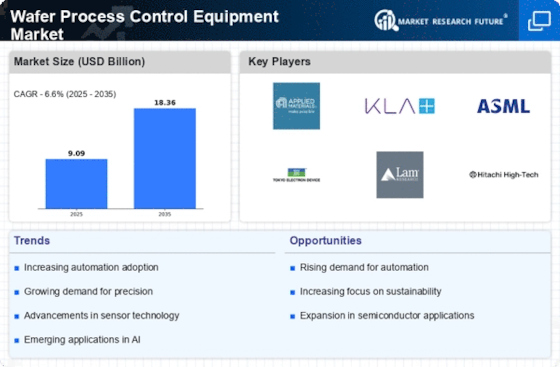
The Wafer Process Control Equipment market is experiencing several noteworthy trends that are shaping the industry's landscape. One prominent trend is the increasing demand for advanced process control solutions to meet the challenges posed by shrinking semiconductor geometries. As semiconductor manufacturers strive to produce smaller and more powerful chips, the need for precise and efficient wafer process control equipment has become paramount. This trend is driving the development of innovative technologies, including advanced metrology tools, inspection systems, and process monitoring solutions, to ensure the high quality and reliability of semiconductor fabrication.
Another significant trend in the market is the rising adoption of Industry 4.0 principles and smart manufacturing practices. Automation, connectivity, and data analytics are becoming integral to wafer process control equipment, allowing for real-time monitoring and control of manufacturing processes. The integration of Internet of Things (IoT) devices and connectivity solutions enables seamless communication between different stages of the manufacturing process, optimizing efficiency, reducing downtime, and enhancing overall productivity.
The market is also witnessing a growing focus on sustainability and environmental responsibility. As industries worldwide place increasing importance on green practices, semiconductor manufacturers are seeking wafer process control equipment that aligns with eco-friendly standards. This trend is driving the development of energy-efficient tools, reduced waste generation, and environmentally conscious manufacturing processes. Companies are actively incorporating sustainability features into their equipment to meet the rising demand for environmentally friendly solutions.
Integration of artificial intelligence (AI) and machine learning (ML) technologies is another prominent trend shaping the Wafer Process Control Equipment market. AI and ML are being employed to enhance the capabilities of process control equipment, enabling predictive maintenance, anomaly detection, and adaptive process control. These technologies contribute to improved efficiency, reduced downtime, and enhanced overall performance, positioning AI and ML as key drivers of innovation in the market.
Moreover, the market is experiencing a shift towards comprehensive solutions that offer end-to-end process control capabilities. Instead of standalone tools, manufacturers are seeking integrated systems that cover multiple aspects of wafer processing, including inspection, metrology, and defect detection. Integrated solutions provide a holistic approach to process control, allowing for better coordination between different stages of semiconductor manufacturing and streamlining overall production workflows.
The increasing complexity of semiconductor devices and the growing demand for heterogeneous integration are driving the trend of multi-functional process control equipment. Manufacturers are developing tools that can handle diverse materials, accommodate various device architectures, and ensure compatibility with advanced packaging techniques. This trend reflects the industry's response to the evolving requirements of modern electronics and the need for versatile process control solutions.
Market consolidation is also a discernible trend in the Wafer Process Control Equipment market. Companies are engaging in mergers and acquisitions to expand their product portfolios, acquire advanced technologies, and strengthen their market presence. This consolidation trend is reshaping the competitive landscape, with larger entities emerging and smaller players aligning to create more robust and diversified offerings.
Furthermore, the semiconductor industry's increasing focus on 3D integration and advanced packaging technologies is influencing the development of wafer process control equipment. As the demand for innovative packaging solutions, such as System-in-Package (SiP) and Fan-Out Wafer-Level Packaging (FO-WLP), rises, manufacturers are investing in process control tools that can address the specific challenges associated with these advanced packaging techniques.
Wafer Process Control Equipment Market Size was valued at USD 9.09 Billion in 2024. The Wafer Process Control Equipment market industry is projected to grow from USD 9.69 Billion in 2025 to USD 17.22 Billion by 2034, exhibiting a compound yearly growth rate (CAGR) of 6.6% during the forecast period (2025 - 2034). Increased demand for higher production yields, improved quality in semiconductor manufacturing, and increasing complexity of semiconductor manufacturing processes are the key market drivers enhancing the market growth.
Source: The Secondary Research, Primary Research, MRFR Database and Analyst Review
Market CAGR for wafer process control equipment is being driven by the rising demand for higher production yields and improved quality in semiconductor manufacturing. Wafer Process Control Equipment enables real-time monitoring and control of various manufacturing parameters, allowing semiconductor manufacturers to optimize their production processes. This optimization is crucial for achieving higher yields by minimizing defects and improving overall efficiency.
The equipment plays a pivotal role in detecting defects and irregularities at various stages of semiconductor production. Early identification of defects allows for prompt corrective actions, reducing the likelihood of faulty products and enhancing the overall quality of the semiconductor components. Wafer Process Control Equipment ensures consistent and precise manufacturing conditions, contributing to the production of semiconductor wafers with uniform quality.
Consistency in product quality is essential for meeting the strict specifications and reliability requirements of modern electronic devices. By minimizing defects and improving process efficiency, Wafer Process Control Equipment helps reduce manufacturing costs associated with material wastage, rework, and lower yields. This cost-effectiveness is a compelling factor for semiconductor manufacturers looking to enhance their competitiveness in the market. As semiconductor technology advances to smaller nodes, such as sub-10nm and beyond, the challenges in maintaining high yields and quality become more pronounced. Wafer Process Control Equipment, equipped with advanced metrology and inspection capabilities, addresses these challenges and supports the successful production of cutting-edge semiconductor devices.
Semiconductor manufacturers strive to maintain a competitive edge by producing high-performance chips with minimal defects. The use of Wafer Process Control Equipment allows company to remain at the forefront of technology, meet market demands for sophisticated electronic devices, and ensure their products meet the growing industry standards. Further, as semiconductor technology advances, the development of smaller and more intricate structures on wafers requires enhanced process control to ensure precision and accuracy in manufacturing. Wafer Process Control Equipment becomes crucial in managing the intricacies of advanced semiconductor processes, driving its growth as a vital component in the production of increasingly sophisticated microelectronics. Thus driving the Wafer Process Control Equipment market revenue.
The Wafer Process Control Equipment Market segmentation, based on product, includes Inspection Equipment, Metrology Equipment, and Process Control Equipment. The inspection equipment segment dominates the market, accounting for the largest market revenue due to its crucial role in ensuring quality and the integrity of semiconductor manufacturing processes.
As semiconductor technology advances, the need for precise inspection becomes increasingly critical to identify defects and irregularities in the production of smaller and more complex semiconductor components. Inspection equipment, such as optical and electron microscopes, allows for high-resolution imaging and analysis, enabling the detection of minute defects that could impact the performance of integrated circuits. The emphasis on quality control and defect detection positions inspection equipment as a cornerstone of Wafer Process Control Equipment, driving its dominance in the market.
The Wafer Process Control Equipment Market segmentation, based on application, includes IDMS, Foundries, and Memory Manufacturers. The foundries category dominates the market due to its central position in semiconductor manufacturing. As specialized facilities responsible for fabricating integrated circuits on behalf of various semiconductor companies, foundries require stringent process control to ensure the quality and the consistency of the wafers they produce. Wafer Process Control Equipment is essential in foundry applications for monitoring and optimizing various stages of semiconductor production, including wafer processing, photolithography, and etching.
The demand for higher production yields and increased efficiency in foundry operations propels the adoption of advanced process control technologies, positioning Wafer Process Control Equipment as a critical component in optimizing manufacturing processes. As the semiconductor industry continues to evolve, the reliance on precise process control in foundries underscores the pivotal role of Wafer Process Control Equipment in sustaining and advancing semiconductor production capabilities.
Source: The Secondary Research, Primary Research, MRFR Database and Analyst Review
By region, the study gives market insights into the North America, Europe, Asia-Pacific, and the Rest of the World. The North American Wafer Process Control Equipment market area dominates this market, the region's strong presence and leadership in semiconductor research, development, and manufacturing. North America is home to some of the world's leading semiconductor companies, research institutions, and technology hubs, contributing to a high demand for cutting-edge wafer process control equipment to maintain technological leadership and innovation.
Further, the prime countries studied in the market report are The US, Canada, Germany, France, the UK, Italy, Spain, Japan, China, India, Australia, South Korea, and Brazil.
Source: The Secondary Research, Primary Research, MRFR Database and Analyst Review
Europe's Wafer Process Control Equipment market accounts for the second-largest market revenue share due to the region's strong emphasis on research and development in semiconductor technology, coupled with the growing demand for the advanced electronics. Further, the German Wafer Process Control Equipment market held the largest market revenue share, and the UK Wafer Process Control Equipment market was the fastest-growing market in the European region.
The Asia-Pacific Wafer Process Control Equipment Market is anticipated to surge at fastest CAGR from the year 2023 to 2032. This is due to the region's strong emphasis on research and development in semiconductor technology, coupled with the growing demand for advanced electronics. Moreover, China’s Wafer Process Control Equipment market held the largest market share, and the Indian Wafer Process Control Equipment market was the fastest-growing market in the Asia-Pacific region.
Leading market players are investing heavily in the research and development in order to expand their product lines, which will help the Wafer Process Control Equipment market grow even more. Market playesr are also undertaking a variety of strategic activities to spread their global footprint, with important market developments including contractual agreements, new product launches, mergers and acquisitions, higher investments, and collaboration with other organizations. To spread and survive in a more competitive and rising market climate, the Wafer Process Control Equipment industry must offer cost-effective items.
Manufacturing locally to minimize the operational costs is one of the key business tactics used by the manufacturers in the global Wafer Process Control Equipment industry to benefit teh clients and increase the market sector. In recent years, the Wafer Process Control Equipment industry has offered some of the most significant advantages to several industries. Major players in the Wafer Process Control Equipment market, including Applied Materials, Inc., KLA Corporation, ASML Holding NV, Hitachi High-Tech Corporation, Thermo Fisher Scientific, ASM Technologies, NXP Semiconductor, Lasertec Corporation, Toray Engineering, Brodcom Inc., and others, are trying to increase market demand by investing in the research and development operations.
Tokyo Electron Ltd. (TEL) is a leading Japanese multinational company specializing in the design, manufacturing, and sale of semiconductor and flat panel display (FPD) production equipment. Headquartered in Tokyo, Japan, TEL plays a pivotal role in the global semiconductor industry by providing cutting-edge solutions for semiconductor manufacturing processes. The company's product portfolio includes equipment for wafer processing, photolithography, deposition, etching, and cleaning, contributing to the development and production of integrated circuits and other advanced semiconductor components. In October 2023, Tokyo Electron Ltd., a Japanese manufacturer of semiconductor manufacturing equipment, and Samsung Electronics Co., Ltd., a South Korean semiconductor manufacturer, signed a Memorandum of Understanding (MoU) in order to collaborate on the development of next-generation wafer process control equipment. The two companies will work together to develop new and innovative equipment that will help to improve the yield and quality of semiconductor manufacturing.
ASML Holding NV is a Dutch multinational company and a global leader in the development and manufacturing of photolithography equipment, which plays a pivotal role in the semiconductor manufacturing process. Headquartered in Veldhoven, Netherlands, ASML is renowned for its advanced lithography machines, particularly its Extreme Ultraviolet (EUV) lithography technology. This technology is crucial for the production of cutting-edge semiconductor components, enabling the fabrication of smaller and more powerful integrated circuits. In September 2023, ASML Holding NV and Intel Corporation, a US semiconductor manufacturer, signed a partnership agreement to develop and commercialize next-generation wafer process control equipment. The two companies will compile their expertise in order to develop new and improved equipment that will help to reduce the cost of semiconductor manufacturing and improve the performance of semiconductor devices.
August 2023: Applied Materials, Inc. and TSMC, a Taiwanese semiconductor manufacturer, signed a partnership agreement to develop and commercialize next-generation wafer process control equipment. The two companies will compile their expertise to develop new and improved equipment that will help TSMC maintain its position as the world's largest contract chip manufacturer.
October 2023: KLA Corporation, a US manufacturer of wafer inspection and metrology equipment, acquired Lam Research Corporation, a US manufacturer of wafer etching equipment, for $10.5 billion. The combined companies will be the world's largest manufacturer of semiconductor capital equipment.
August 2023: Lam Research Corporation (LRCX) and TSMC (TSMC) announced a partnership to develop next-generation semiconductor manufacturing technology. The two companies will work together to develop new technologies that will enable the production of more advanced semiconductors.
© 2024 Market Research Future ® (Part of WantStats Reasearch And Media Pvt. Ltd.)