• Cat-intel
  • MedIntelliX
  • Resources
  • About Us
  • Request Free Sample ×

    Kindly complete the form below to receive a free sample of this Report

    Leading companies partner with us for data-driven Insights

    clients tt-cursor
    Hero Background

    GaN Substrate Wafer Market

    ID: MRFR/SEM/38283-HCR
    128 Pages
    Aarti Dhapte
    October 2025

    GaN Substrate and Wafer Market Research Report By Application (Power Electronics, Radio Frequency Devices, Optoelectronics, LEDs), By Wafer Size (2-inch, 4-inch, 6-inch, 8-inch), By Type (Bulk GaN, Epitaxial GaN, GaN on Silicon, GaN on Sapphire), By End Use Industry (Consumer Electronics, Telecommunications, Aerospace and Defense, Energy and Power) and By Regional (North America, Europe, South America, Asia Pacific, Middle East and Africa) – Industry Forecast to 2035

    Share:
    Download PDF ×

    We do not share your information with anyone. However, we may send you emails based on your report interest from time to time. You may contact us at any time to opt-out.

    GaN Substrate Wafer Market Infographic
    Purchase Options

    GaN Substrate Wafer Market Summary

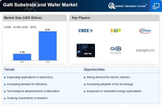
    The Global GaN Substrate and Wafer Market is projected to grow significantly from 1.35 USD Billion in 2024 to 6.01 USD Billion by 2035.

    Key Market Trends & Highlights

    GaN Substrate and Wafer Key Trends and Highlights

    • The market is expected to witness a compound annual growth rate (CAGR) of 14.54% from 2025 to 2035.
    • By 2035, the market valuation is anticipated to reach 6.01 USD Billion, indicating robust growth potential.
    • in 2024, the market is valued at 1.35 USD Billion, reflecting the increasing demand for GaN technology.
    • Growing adoption of GaN technology due to its efficiency and performance advantages is a major market driver.

    Market Size & Forecast

    2024 Market Size 1.35 (USD Billion)
    2035 Market Size 6.01 (USD Billion)
    CAGR (2025-2035) 14.53%

    Major Players

    Qorvo, Texas Instruments, ON Semiconductor, Infineon Technologies, Samsung Electronics, Wolfspeed, Microsemi, Nichia Corporation, Fuji Electric, Vishay Intertechnology, Toshiba Corporation, StMicroelectronics, Mitsubishi Electric, Broadcom, NXP Semiconductors

    GaN Substrate Wafer Market Trends

    The GaN Substrate and Wafer Market is experiencing significant growth due to key market drivers, such as the rising demand for energy-efficient devices and advancements in semiconductor technology. As industries prioritize sustainability, GaN technology offers advantages in terms of higher efficiency and reduced energy consumption. The demand for electric vehicles and renewable energy sources is also pushing the adoption of GaN substrates, as they improve performance in power electronics. Additionally, the increasing need for high-frequency and high-temperature applications in telecommunications and aerospace sectors further fuels the market for GaN wafers.In terms of opportunities, there are several avenues for exploration.

    The expanding consumer electronics sector presents a fertile ground for GaN technology, particularly in developing compact and lightweight devices with enhanced performance. 

    Emerging markets are also showing interest in adopting GaN technology, paving the way for new entrants. Collaboration between research institutions and manufacturers can lead to innovative solutions, further capturing the growing market. As industries continue to evolve, there is room for GaN technology to penetrate various applications that were previously dominated by silicon-based materials. Recent trends indicate a shift toward more integrated solutions and the development of new fabrication techniques, which enhance the overall efficiency and reliability of GaN substrates.The focus on creating scalable manufacturing processes is gaining importance, ensuring that production can meet the increasing demand.

    Investments in R are critical as companies strive to improve material quality and performance metrics. Moreover, the potential for GaN technology to be utilized in high-performance computing indicates a future direction for the market. Overall, the landscape of the GaN Substrate and Wafer Market continues to evolve, driven by innovation and an increasing awareness of power efficiency.

    Source: Primary Research, Secondary Research, MRFR Database and Analyst Review

    The ongoing advancements in GaN technology are poised to revolutionize the semiconductor landscape, enhancing efficiency and performance across a myriad of applications.

    U.S. Department of Energy

    GaN Substrate Wafer Market Drivers

    Market Growth Projections

    The Global GaN Substrate and Wafer Market Industry is projected to experience substantial growth over the next decade. With a market value of 1.35 USD Billion in 2024, the industry is expected to reach 6.01 USD Billion by 2035, reflecting a robust compound annual growth rate (CAGR) of 14.54% from 2025 to 2035. This growth trajectory indicates a strong demand for GaN technology across various sectors, including telecommunications, automotive, and renewable energy. The increasing focus on energy efficiency and high-performance electronics is likely to drive further investments in GaN substrates and wafers, solidifying their position in the global semiconductor landscape.

    Government Initiatives and Funding

    Government initiatives aimed at promoting semiconductor manufacturing and research play a crucial role in shaping the Global GaN Substrate and Wafer Market Industry. Various countries are investing in GaN technology to enhance their technological capabilities and reduce reliance on foreign semiconductor supplies. For instance, funding programs and incentives for research and development in GaN applications are likely to accelerate innovation and commercialization. These initiatives not only foster a conducive environment for market growth but also align with national strategies to strengthen domestic semiconductor industries, thereby driving the demand for GaN substrates and wafers.

    Rising Demand for Power Electronics

    The Global GaN Substrate and Wafer Market Industry experiences a surge in demand for power electronics, driven by the increasing adoption of electric vehicles and renewable energy systems. GaN technology offers superior efficiency and performance compared to traditional silicon-based solutions, making it a preferred choice for power conversion applications. As industries transition towards greener technologies, the market is projected to reach 1.35 USD Billion in 2024, reflecting a robust growth trajectory. The shift towards energy-efficient devices is likely to further bolster the demand for GaN substrates and wafers, positioning the industry for sustained expansion.

    Emerging Markets and Global Expansion

    Emerging markets present significant opportunities for the Global GaN Substrate and Wafer Market Industry, as countries in Asia-Pacific and Latin America ramp up their semiconductor manufacturing capabilities. The growing industrial base in these regions, coupled with increasing investments in technology, is likely to drive demand for GaN substrates and wafers. As these markets develop, they may adopt GaN technology for various applications, including automotive and industrial sectors. This expansion into new geographical areas could further enhance the industry's growth prospects, contributing to a more diversified global market landscape.

    Growing Applications in 5G Technology

    The proliferation of 5G technology significantly impacts the Global GaN Substrate and Wafer Market Industry, as GaN materials are essential for high-frequency and high-power applications. The deployment of 5G networks necessitates advanced semiconductor solutions capable of handling increased data traffic and improving signal integrity. GaN technology, with its superior performance characteristics, is poised to play a pivotal role in the development of 5G infrastructure. As the global rollout of 5G continues, the market is expected to expand, potentially reaching 6.01 USD Billion by 2035, driven by the increasing demand for efficient and reliable communication systems.

    Advancements in Semiconductor Technology

    Technological advancements in semiconductor manufacturing processes significantly influence the Global GaN Substrate and Wafer Market Industry. Innovations such as improved epitaxial growth techniques and enhanced wafer fabrication methods contribute to higher yield rates and reduced production costs. These advancements facilitate the integration of GaN technology into various applications, including telecommunications and consumer electronics. As a result, the market is expected to witness a compound annual growth rate (CAGR) of 14.54% from 2025 to 2035, indicating a strong potential for growth driven by continuous improvements in semiconductor technology.

    Market Segment Insights

    GaN Substrate and Wafer Market Application Insights

    The GaN Substrate and Wafer Market is witnessing noteworthy growth, particularly across its various applications, namely Power Electronics, Radio Frequency Devices, Optoelectronics and LEDs. As of 2023, the overall market achieved a valuation of 1.03 USD Billion, with Power Electronics emerging as the leading application, valued at 0.4 USD Billion, and projected to expand to 1.4 USD Billion by 2032.

    This segment's prominence can be attributed to the increasing demand for efficient power conversion solutions in sectors such as automotive and consumer electronics, where energy efficiency is paramount.Following closely, Radio Frequency Devices accounted for 0.25 USD Billion in 2023 and is expected to grow to 0.85 USD Billion by 2032, highlighting its vital role in telecommunications, where high-frequency performance is essential. 

    The Optoelectronics application, which includes devices like lasers and photodetectors, has a valuation of 0.2 USD Billion in 2023, with projections to reach 0.7 USD Billion by 2032, indicating its significance in fields such as data communications and medical imaging.

    Meanwhile, the LEDs application, valued at 0.18 USD Billion in 2023 with a forecasted growth to 0.55 USD Billion by 2032, reflects the continuing demand for energy-efficient lighting solutions, driven by both consumer and commercial sectors.The majority holding of Power Electronics within the GaN Substrate and Wafer Market revenue underscores its critical importance, making it a significant driver of market growth amid rising energy consumption concerns.

    Overall, the growth drivers across these segments are strongly dictated by technological advancements and a shift towards sustainable energy practices, while challenges may arise from competition in semiconductor technologies and the ensuring need for complementary materials and processes. Thus, the GaN Substrate and Wafer Market segmentation highlights distinct application areas that not only contribute to overall market statistics but also reshape industry expectations and opportunities for future development.

    GaN Substrate and Wafer Market Wafer Size Insights

    Within this segment, various sizes, including 2-inch, 4-inch, 6-inch and 8-inch, each possess unique advantages that cater to different technological requirements. The 2-inch wafers are often favored for their cost-effectiveness in small-scale applications, while the 4-inch wafers provide a balance of size and performance, making them widely used in production.The 6-inch wafers are gaining traction due to their ability to deliver higher output with reduced costs per unit, making them appealing to manufacturers focusing on efficiency. The 8-inch wafers dominate the market by enabling the highest production volume, thus supporting large-scale applications in sectors such as telecommunications and power electronics.

    Overall, the GaN Substrate and Wafer Market data showcases a trend toward larger wafer sizes as the technology evolves, driven by increasing demands for power efficiency and the miniaturization of components.

    GaN Substrate and Wafer Market Type Insights

    This segment is intricately divided among various types, including Bulk GaN, Epitaxial GaN, GaN on Silicon and GaN on Sapphire. Each type plays a pivotal role in the market landscape. Bulk GaN is often favored for high-power applications due to its superior thermal conductivity, while Epitaxial GaN is recognized for its ability to provide high electron mobility and efficiency, making it crucial for advanced electronic devices.GaN on Silicon is gaining traction due to its cost-effectiveness and compatibility with existing silicon technologies, catering to a broad spectrum of applications.

    Meanwhile, GaN on Sapphire remains significant for optoelectronic applications, especially in LEDs and laser diodes, contributing to the overall growth dynamics. The GaN Substrate and Wafer Market revenue reflects these trends, with increasing demand driven by the rise in electric vehicles, renewable energy systems and advanced communication technologies. However, challenges such as material defectiveness and high manufacturing costs persist, presenting a mixed landscape of opportunities and difficulties in market expansion.

    GaN Substrate and Wafer Market End Use Industry Insights

    The GaN Substrate and Wafer Market is experiencing substantial growth, particularly within the End Use Industry segment, which encompasses vital sectors such as Consumer Electronics, Telecommunications, Aerospace and Defense and Energy and Power. The Consumer Electronics sector plays a crucial role as it continues to leverage GaN technology for more efficient power converters and faster charging devices.Meanwhile, the Telecommunications industry significantly benefits from the high-performance capabilities of GaN substrates, enhancing signal quality and data speeds in 5G technology. The Aerospace and Defense sector demands high reliability and performance, making GaN a preferred choice for various military and space applications.

    Energy and Power is also a significant area, as GaN technology supports the transition to more sustainable energy sources and enhances power efficiency in renewable applications. As the GaN Substrate and Wafer Market evolves, these industries will drive competitive advantage through innovation and improved efficiency, contributing to the overall market growth.

    Get more detailed insights about GaN Substrate Wafer Market

    Regional Insights

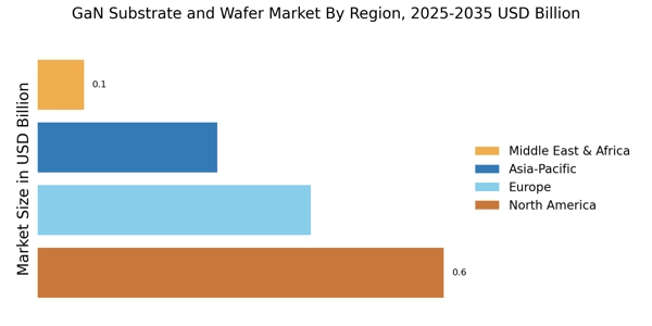
    The GaN Substrate and Wafer Market is experiencing notable growth, driven by increasing demand in various applications. In 2023, North America accounted for a valuation of 0.35 USD Billion, demonstrating significant market presence with a projected increase to 1.15 USD Billion by 2032, thus holding a majority share in the industry. Europe follows with a market value of 0.25 USD Billion in 2023, expected to grow to 0.9 USD Billion by 2032, reflecting consistent development.

    The APAC region mirrors this trend with a valuation of 0.35 USD Billion in 2023, rising to 1.25 USD Billion by 2032, showcasing its importance in global supply chains and manufacturing.South America and the MEA regions, though smaller in comparison, show potential with market valuations of 0.05 USD Billion and 0.03 USD Billion in 2023, respectively. The collective increase across these regions indicates a robust market growth opportunity driven by technological advancements and the growing application of GaN technology in electronics, renewable energies and telecommunications.

    The diversification in demand across these regions emphasizes their strategic importance in the GaN Substrate and Wafer Market, contributing to its overall growth and industry dynamics.

    GaN Substrate and Wafer Market Regional Insights

    Source: Primary Research, Secondary Research, MRFR Database and Analyst Review

    Key Players and Competitive Insights

    The GaN Substrate and Wafer Market represents a rapidly evolving segment in the semiconductor industry characterized by innovation and heightened competition. Gallium Nitride (GaN) technology is widely recognized for its superior performance in power electronics and radio frequency applications, which has driven a surge in demand for GaN substrates and wafers. This market is marked by the presence of a diverse range of players, each vying for market share through innovation, strategic partnerships, and advancements in manufacturing processes.

    Key trends include an increasing focus on miniaturization, energy efficiency and enhanced thermal management, which are propelling the adoption of GaN materials across various applications. 

    As economies worldwide transition to more sustainable and energy-efficient technologies, the importance of GaN substrates and wafers is expected to grow, further intensifying competition among existing market players and attracting new entrants.Qorvo stands out within the GaN Substrate and Wafer Market due to its robust portfolio and strong commitment to research and development. The company has established itself as a leader with its high-performance GaN solutions tailored for diverse applications, particularly in the market for mobile connectivity and advanced radar systems.

    Qorvo's significant investment in innovation has resulted in advanced materials technology, allowing for the manufacture of specialized GaN substrates and wafers that facilitate improved efficiency and performance in semiconductor devices. With a solid reputation for reliability and product quality, Qorvo has also developed strategic partnerships that enhance its market presence, further reinforcing its competitive advantage within the sector.

    The company’s ability to address customer-specific needs through customized solutions has solidified its standing in the industry, enabling it to capture a substantial share of the growing GaN market.Texas Instruments holds a prominent position in the GaN Substrate and Wafer Market, driven by its extensive expertise in analog and embedded processing technologies. 

    The company is well-regarded for its commitment to bringing cutting-edge GaN solutions to a wide range of applications, particularly in power management and signal processing. Texas Instruments leverages its strong engineering capabilities and vast resources to enhance the performance and efficiency of its GaN products. The company’s strategic focus on innovation ensures that it remains competitive, as evidenced by its continued investment in research and development. Additionally, Texas Instruments maintains a robust supply chain and distribution network, facilitating the widespread availability of its products to meet the demands of various industries.

    By staying at the forefront of GaN technology developments, Texas Instruments is well-positioned to capitalize on the growing market opportunities presented by the increasing adoption of GaN solutions for energy-efficient applications.

    Key Companies in the GaN Substrate Wafer Market market include

    Industry Developments

    In recent months, the GaN Substrate and Wafer Market has seen significant activity, particularly among key players such as Qorvo, Texas Instruments, ON Semiconductor, Infineon Technologies, and Samsung Electronics. The demand for GaN technology is surging due to its applications in high-efficiency power amplifiers and RF devices, driving innovations that enhance performance while reducing size and weight. Wolfspeed and Microsemi are actively expanding production capabilities to meet the increasing market needs, while Nichia Corporation is investing in RD for advanced GaN semiconductor applications.

    Mergers and acquisitions are shaping the competitive landscape, with notable transactions involving Mitsubishi Electric and Broadcom, which are enhancing their technological portfolios and market reach. The recent collaboration between NXP Semiconductors and various universities aims to push forward research into new GaN materials, facilitating faster developments in the semiconductor sector. The overall growth in market valuations for these companies is indicative of escalating investor confidence and expanding opportunities in electronic applications, particularly in electric vehicles and renewable energy setups, which further bolster demand for GaN substrates and wafers.

    Future Outlook

    GaN Substrate Wafer Market Future Outlook

    The GaN Substrate and Wafer Market is poised for growth at 14.53% CAGR from 2025 to 2035, driven by advancements in power electronics and increasing demand for efficient energy solutions.

    New opportunities lie in:

    • Invest in R&D for next-gen GaN materials to enhance performance and reduce costs.
    • Develop strategic partnerships with semiconductor manufacturers to expand market reach.
    • Explore applications in electric vehicles and renewable energy sectors for innovative product offerings.

    By 2035, the GaN Substrate and Wafer Market is expected to achieve substantial growth, solidifying its position as a key player in advanced technologies.

    Market Segmentation

    GaN Substrate and Wafer Market Type Outlook

    • Bulk GaN
    • Epitaxial GaN
    • GaN on Silicon
    • GaN on Sapphire

    GaN Substrate and Wafer Market Regional Outlook

    • North America
    • Europe
    • South America
    • Asia Pacific
    • Middle East and Africa

    GaN Substrate and Wafer Market Wafer Size Outlook

    • 2-inch
    • 4-inch
    • 6-inch
    • 8-inch

    GaN Substrate and Wafer Market Application Outlook

    • Power Electronics
    • Radio Frequency Devices
    • Optoelectronics
    • LEDs

    GaN Substrate and Wafer Market End Use Industry Outlook

    • Consumer Electronics
    • Telecommunications
    • Aerospace and Defense
    • Energy and Power

    Report Scope

    Report Attribute/Metric Details
    Market Size 2024 USD 1.35 Billion
    Market Size 2025 USD 1.55 Billion
    Market Size 2035 6.01 (USD Billion)
    Compound Annual Growth Rate (CAGR) 14.53% (2025 - 2035)
    Base Year 2024
    Market Forecast Period 2025 - 2035
    Historical Data 2020-2023
    Market Forecast Units USD Billion
    Key Companies Profiled Qorvo, Texas Instruments, ON Semiconductor, Infineon Technologies, Samsung Electronics, Wolfspeed, Microsemi, Nichia Corporation, Fuji Electric, Vishay Intertechnology, Toshiba Corporation, StMicroelectronics, Mitsubishi Electric, Broadcom, NXP Semiconductors
    Segments Covered Application, Wafer Size, Type, End Use Industry, Regional
    Key Market Opportunities Rising demand for electric vehicles, Growth in 5G infrastructure, Advancements in semiconductor technology, Increased investment in renewable energy, Expanding consumer electronics sector
    Key Market Dynamics Rising demand for electric vehicles, Increasing adoption of renewable energy, Advances in semiconductor technology, Growing consumer electronics market, Cost reduction in manufacturing processes
    Countries Covered North America, Europe, APAC, South America, MEA

    FAQs

    What is the expected market size of the GaN Substrate and Wafer Market by 2035?

    The GaN Substrate and Wafer Market is expected to reach a value of 5.25 USD Billion by 2035.

    What is the compound annual growth rate (CAGR) for the GaN Substrate and Wafer Market during the forecast period?

    The market is projected to grow at a CAGR of 14.53% from 2025 to 2035.

    Which region is anticipated to have the largest market share in the GaN Substrate and Wafer Market by 2032?

    North America is anticipated to have the largest market share, valued at 1.15 USD Billion by 2032.

    What is the expected market value for the Power Electronics segment by 2032?

    The Power Electronics segment is expected to be valued at 1.4 USD Billion by 2032.

    What are the projected market values for the Radio Frequency Devices segment by 2032?

    The Radio Frequency Devices segment is projected to be valued at 0.85 USD Billion by 2032.

    Who are the key players in the GaN Substrate and Wafer Market?

    Key players include Qorvo, Texas Instruments, ON Semiconductor, Infineon Technologies and Samsung Electronics.

    What will the market value for the Optoelectronics segment be by 2032?

    The Optoelectronics segment is expected to reach a market value of 0.7 USD Billion by 2032.

    What is the expected market size for the MEA region by 2032?

    The MEA region is expected to reach a market size of 0.1 USD Billion by 2032.

    What is the projected market size for the LED segment by 2032?

    The LEDs segment is projected to be valued at 0.55 USD Billion by 2032.

    What is the expected market value for Europe in the GaN Substrate and Wafer Market by 2032?

    Europe is expected to reach a market value of 0.9 USD Billion by 2032.

    Download Free Sample

    Kindly complete the form below to receive a free sample of this Report

    Case Study
    Chemicals and Materials