info@marketresearchfuture.com   ๐Ÿ“ž  +1 (855) 661-4441(US)   ๐Ÿ“ž  +44 1720 412 167(UK)
Certified Global Research Member
Isomar fd.webp Wcrc 57.webp
Key Questions Answered
  • Global Market Outlook
  • In-depth analysis of global and regional trends
  • Analyze and identify the major players in the market, their market share, key developments, etc.
  • To understand the capability of the major players based on products offered, financials, and strategies.
  • Identify disrupting products, companies, and trends.
  • To identify opportunities in the market.
  • Analyze the key challenges in the market.
  • Analyze the regional penetration of players, products, and services in the market.
  • Comparison of major players financial performance.
  • Evaluate strategies adopted by major players.
  • Recommendations
Why Choose Market Research Future?
  • Vigorous research methodologies for specific market.
  • Knowledge partners across the globe
  • Large network of partner consultants.
  • Ever-increasing/ Escalating data base with quarterly monitoring of various markets
  • Trusted by fortune 500 companies/startups/ universities/organizations
  • Large database of 5000+ markets reports.
  • Effective and prompt pre- and post-sales support.

GaN on Si EPI wafers Market Research Report Information By Structure (Lateral GaN on Si, Vertical GaN on Si, and Hybrid GaN on Si), By Application (Low power applications, medium power applications, High power applications, and Very high power applications), By Procurement model (Tender based and direct purchase), By Industry Vertical (IT & Telecom, Consumer electronics, Automotive, Aerospace & Defense, Others) And By Region (North America, Europe, Asia-Pacific, Middle East & Africa, And South America) โ€“Industry Forecast Till 2032


ID: MRFR/SEM/19773-CR | 128 Pages | Author: Aarti Dhapte| March 2024

Global GaN on Si EPI wafers Market Overview


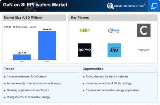
GaN on Si EPI wafers Market Size was valued at USD 1,146.1 million in 2022. The GaN on Si EPI wafers market industry is projected to grow from USD 1,344.2 million in 2023 to USD 5,374.8 million by 2032, exhibiting a compound annual growth rate (CAGR) of 16.6% during the forecast period (2024 - 2032). Increasing demand for higher power density power electronics, Growing demand for wireless charging, huge demand from consumer electronics and automotive sector are the key market drivers boosting the growth of the GaN on Si EPI wafers market.


GaN on Si EPI wafers Market Overview


Source: Secondary Research, Primary Research, MRFR Database, and Analyst Review


GaN on Si EPI Wafers Market Trends


  • INCREASING DEMAND FOR HIGHER POWER DENSITY POWER ELECTRONICS


The increasing demand for higher power density power electronics is considered a key driver for the GaN on Si EPI wafer market. One of the main drivers of the GaN on Si EPI wafer market is the trend towards miniaturization of electronic devices and increasing demand for high-performance electronic products. As electronic devices become smaller and more complex, there is a growing need for more compact and efficient power electronics. GaN on Si EPI wafers offer higher power density and efficiency compared to traditional silicon-based power electronics, making them ideal for high-power applications that require smaller and more efficient power electronics. Another driver of the GaN on Si EPI wafer market is the growing demand for 5G technology. 5G technology requires higher frequency and faster data rates than previous generations of wireless technology, which in turn requires the use of new materials and technologies such as GaN. GaN is already being used in RF applications, and its use in 5G technology is expected to increase significantly in the coming years.


GaN on Si EPI Wafers Market Segment Insights


GaN on Si EPI Wafers Structure Insights


The GaN on Si EPI wafers market in this report has been segmented on the basis of Structure into 3 types, namely Lateral GaN on Si, Vertical GaN on Si and Hybrid GaN on Si.


Lateral GaN on Si holds the largest market share which is 40.2% while the second largest share is held by vertical GaN on Si. Lateral GaN on Si EPI wafers are a type of semiconductor wafer used in the production of lateral GaN devices. These wafers feature a Gallium Nitride (GaN) layer grown on a Silicon (Si) substrate using an epitaxial process. The lateral design refers to the layout of the GaN transistors or devices, where the current flows horizontally along the surface of the wafer. While vertical GaN on Si EPI wafers are a type of semiconductor wafer used in the production of vertical GaN devices. These wafers feature a Gallium Nitride (GaN) layer grown on a Silicon (Si) substrate using an epitaxial process. The vertical design refers to the structure of the GaN devices, where the current flows vertically through the layers of the wafer.


GaN on Si EPI Wafers Applications Insights


The GaN on Si EPI wafers Market, in this report, has been segmented on the basis of Application into low-power applications, medium-power applications, high-power applications, very high-power applications.


Low-power applications is further segmented into AC-DC adapters for laptops and other electronic devices, USB-PD chargers, Wireless charging pads, and others. Medium-Power Applications is segmented into LED lighting power supplies, AC-DC converters, Power supplies for electronic appliances, and others. High-Power Applications is segmented into Electric vehicle (EV) power converters, Motor drives, Power converters, and others. Very-High Power Applications is segmented into Grid-tied inverters for utility-scale solar and wind power plants, Traction inverters, Power converters, and others.


Very high-power application segment holds the largest market share, and it is 32.5% as of 2022 while high power applications segment holds the second largest market share. GaN on Si EPI wafers excel in very high-power applications, where extreme power handling capabilities, high efficiency, and reliability are critical. These wafers enable the development of devices that can handle the most demanding power requirements and outperform traditional silicon-based solutions. While, GaN on Si EPI wafers are particularly well-suited for high-power applications, where superior power handling capabilities, high efficiency, and robustness are crucial. These wafers enable the development of high-power devices that outperform traditional silicon-based solutions.


GaN on Si EPI Wafers Procurement model Insights


The GaN on Si EPI wafers Market, in this report, has been segmented on the basis of Procurement model into Tender Based and Direct Purchase. The direct purchase segment holds the largest market share which is 64.6% while the tender based segment holds 35.4% share as of 2022.


FIGURE 1: GaN on Si EPI wafers Market, By Procurement Model, 2019-2032 (USD MILLION)


GaN on Si EPI wafers Market, By Procurement Model, 2019-2032


Source: Secondary Research, Primary Research, MRFR Database, and Analyst Review


Direct purchase is a procurement model commonly used for acquiring GaN on Si EPI wafers in various industries. In this procurement method, organizations directly approach suppliers and negotiate the terms and conditions of the purchase without soliciting competitive bids or proposals.


Tender-based procurement is a commonly employed model for acquiring GaN on Si EPI wafers in various industries. In this procurement method, organizations issue a formal request for suppliers to submit competitive bids or proposals to fulfill their GaN on Si EPI wafer requirements. The tender process begins with the organization issuing a detailed tender document that outlines the specifications, quantity, quality requirements, delivery schedule, and other terms and conditions.


GaN on Si EPI Wafers Industry Verticals Insights


The GaN on Si EPI wafers market in this report has been segmented on the basis of It & Telecom, consumer electronics, safety and security, automotive, aerospace and defense, and others. Consumer electronics holds the second largest share, which is 19.9% while others segment holds the largest market share.


Consumer electronics is a prominent industry vertical that heavily relies on GaN on Si EPI wafers for the development of innovative and high-performance devices. GaN on Si EPI wafers offer numerous advantages that cater to the evolving needs of the consumer electronics market. In the consumer electronics sector, GaN on Si EPI wafers are utilized in various applications such as power adapters, chargers, inverters, LED lighting, and audio systems. The high-power density, improved efficiency, and compact form factor of GaN-based devices enable the design of sleeker and more energy-efficient consumer electronic products.


The applications of GaN on Si EPI wafers extend beyond the previously mentioned industry verticals. There are several other industry sectors where GaN on Si EPI wafers find significant utility and foster technological advancements. One such industry vertical is the renewable energy sector. GaN on Si EPI wafers are employed in renewable energy systems such as solar inverters and wind power converters. The high efficiency and power handling capabilities of GaN-based devices contribute to improved energy conversion and grid integration, enabling the widespread adoption of renewable energy sources. Another industry vertical is the medical sector, where GaN on Si EPI wafers are utilized in medical imaging equipment, ultrasound systems, and various medical devices. GaN-based solutions offer enhanced imaging quality, higher signal resolution, and improved device performance, contributing to more accurate diagnoses and advanced medical procedures.


GaN on Si EPI Wafers Regional Insights


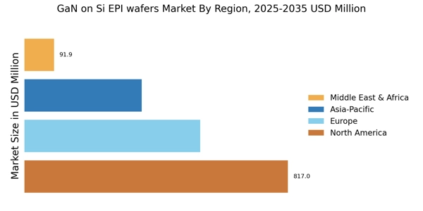
Based on Region, the global GaN on Si EPI wafers is segmented into North America, Europe, Asia-Pacific, Middle East & Africa, and South America. Asia-Pacific holds the largest market share, which is 44.1% of the total share while North America holds the second largest market share which is 29.3% of the total share.


North America has been further segmented into the US, Canada, and Mexico. North America accounts for one of the largest market shares in the GaN on Silicon for power market due to the presence of notable GaN on Silicon companies such as Texas Instruments Incorporated, NXP USA Inc and many others. The major players in the GaN market have been working on the technology for over 15 years and have amassed a sizable body of knowledge, skill, and competence. But most importantly, they have developed an almost fervent feeling of faith in technology's long-term potential.


Asia-Pacific has been further segmented into China, Japan, India, and the Rest of Asia-Pacific. Asia-Pacific is another promising market for GaN on Si for power. Asia-Pacific is a center for automotive, aerospace, and semiconductor technology. Due to rapidly expanding markets for energy-efficient electronics, China, India, and Japan account for large shares in the area. The rapidly developing semiconductor market is one of the major factors which drives the growth of GaN on Si for power in the Asia-Pacific region.


FIGURE 2: GAN ON SI EPI WAFERS MARKET SIZE BY REGION 2022 VS 2032


GAN ON SI EPI WAFERS MARKET SIZE BY REGION 2022 VS 2032


Source: Secondary Research, Primary Research, MRFR Database, and Analyst Review


GaN on Si EPI Wafers Market Key Players and Competitive Insights


With a strong presence across different verticals and geographies, the GaN on Si EPI Wafers market is highly competitive and dominated by established, pure-play vendors. Over 12 vendors cater to this market, and they continually innovate their solutions to meet the evolving needs of businesses by adopting new technologies. These vendors have a robust geographic footprint and partner ecosystem to cater to diverse customer segments. The GaN on Si EPI Wafers market is highly competitive, with many vendors offering similar products and services.


The major players in the market include Infineon Technologies, Texas Instruments Incorporated, Toshiba Corporation, Panasonic Corporation, NexGen Power Systems, Efficient Power Conversion Corporation, STMICROELECTRONICS, Navitas Semiconductor Corporation, NEXPERIA, Semiconductor Components Industries, Llc, Rohm Company Ltd, Broadcom Inc, MACOM Technology Solutions Inc, WOLFSPEED, INC, X-FAB Silicon Foundries SE, NXP Semiconductors, Renesas Electronics Corp, VisIC Technologies Ltd, Qorvo Inc.


Key Companies in the GaN on Si EPI Wafers market include


  • Infineon Technologies

  • Texas Instruments Incorporated

  • Toshiba Corporation

  • Panasonic Corporation

  • NexGen Power Systems

  • Efficient Power Conversion Corporation

  • STMICROELECTRONICS

  • Navitas Semiconductor Corporation


GaN on Si EPI Wafers Industry Developments


March 2023: EPC has collaborated with SHARGE Technology (SHARGE) to create a 67 W USB PD charger with a power display panel. The Retro 67 fast charger employs EPC's 100 V GaN FET, EPC2218, which can generate 231 A pulsed current in a 3.5 mm x 1.95 mm footprint, providing designers with a substantially smaller, more efficient device than silicon MOSFET for USB PD fast chargers.


April 2023: Navitas Semiconductor has made a agreement with distribution deal with Mouser Electronics. Mouser will stock Navitas GanFast and GeneSiC wide bandgap (WBG) semiconductor technology under the new global partnership. GaNFast power integrated circuits (ICs) combine gallium nitride (GaN) power and drive with control, sensing, and protection to provide quicker charging, higher power density, and greater energy savings.


April 2023: ZF and Wolfspeed announced their collaboration on upcoming silicon carbide semiconductor devices. The cooperation also involves a sizeable investment from ZF to help finance the development of the largest and most sophisticated 200mm silicon carbide device fab in Ensdorf, Germany.


GaN on Si EPI Wafers Market Segmentation


GaN on Si EPI Wafers Structure Outlook


  • Lateral GaN on Si

  • Vertical GaN on Si

  • Hybrid GaN on Si


GaN on Si EPI Wafers Applications Outlook


  • Low power applications

  • Medium power applications

  • High power applications

  • Very high-power applications


GaN on Si EPI Wafers Procurement Model Outlook


  • Tender based

  • Direct purchase


GaN on Si EPI Wafers Industry Vertical Outlook


  • IT & telecom

  • Consumer electronics

  • Automotive

  • Aerospace and defense

  • others


GaN on Si EPI Wafers Regional Outlook


  • North America

    • US

    • Canada

    • Mexico


  • Europe

    • Germany

    • France

    • UK

    • Italy

    • Spain

    • Rest of Europe


  • Asia-Pacific

    • China

    • Japan

    • India

    • Australia

    • South Korea

    • Australia

    • Rest of Asia-Pacific


  • Middle East & Africa

  • South America

Report Attribute/Metric Details
Market Size 2022 USD 1,146.1 Million
Market Size 2023 USD 1,344.2 Million
Market Size 2032 USD 5,374.8 Million
Compound Annual Growth Rate (CAGR) 16.6% (2024-2032)
Base Year 2023
Market Forecast Period 2024-2032
Historical Data 2018- 2022
Market Forecast Units Value (USD Million)
Report Coverage Revenue Forecast, Market Competitive Landscape, Growth Factors, and Trends
Segments Covered Procurement model, applications, structure, Industry vertical
Geographies Covered Europe, North America, Asia-Pacific, and the South America, Middle East & Africa
Countries Covered The U.S, Germany, Canada, U.K., Italy, France, Spain, Japan, China, Australia, India, South Korea, and Brazil
Key Companies Profiled Infineon Technologies, Texas Instruments Incorporated, Toshiba Corporation, Panasonic Corporation, NexGen Power Systems, Efficient Power Conversion Corporation, STMICROELECTRONICS, Navitas Semiconductor Corporation, NEXPERIA, Semiconductor Components Industries, Llc, Rohm Company Ltd, Broadcom Inc, MACOM Technology Solutions Inc, WOLFSPEED, INC, X-FAB Silicon Foundries SE,
Key Market Opportunities ยทย ย ย ย ย ย  Growing adoption electronic vehicles and hybrid EVs ยทย ย ย ย ย ย  Increasing use in 5G infrastructure
Key Market Dynamics ยทย ย ย ย ย ย  Increasing demand for higher power density power electronics


Frequently Asked Questions (FAQ) :

The GaN on Si EPI wafers Market size is expected to be valued at USD 1,146.1 Million in 2022.

The global market is projected to grow at a CAGR of 16.6% during the forecast period, 2024-2032.

Asia-Pacific had the largest share of the global market.

The key players in the market are Infineon Technologies, Texas Instruments Incorporated, Toshiba Corporation, Panasonic Corporation, NexGen Power Systems, Efficient Power Conversion Corporation, STMICROELECTRONICS, Navitas Semiconductor Corporation, NEXPERIA.

Leading companies partner with us for data-driven Insights.

client_1 client_2 client_3 client_4 client_5 client_6 client_7 client_8 client_9 client_10

Kindly complete the form below to receive a free sample of this Report

Please fill in Business Email for Quick Response

We do not share your information with anyone. However, we may send you emails based on your report interest from time to time. You may contact us at any time to opt-out.

Purchase Option
Single User $ 4,950
Multiuser License $ 5,950
Enterprise User $ 7,250
Compare Licenses
Tailored for You
  • Dedicated Research on any specifics segment or region.
  • Focused Research on specific players in the market.
  • Custom Report based only on your requirements.
  • Flexibility to add or subtract any chapter in the study.
  • Historic data from 2014 and forecasts outlook till 2040.
  • Flexibility of providing data/insights in formats (PDF, PPT, Excel).
  • Provide cross segmentation in applicable scenario/markets.