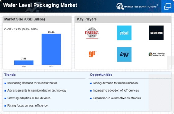
Wafer Level Packaging Market Size was valued at USD 4.7 Billion in 2022. The wafer level packaging industry is projected to grow from USD 5.6 Billion in 2023 to USD 23.007 Billion by 2032, exhibiting a compound annual growth rate (CAGR) of 19.30% during the forecast period (2024 - 2032). Rapid advancements in the semiconductor industry, widespread use of consumer electronics, and rising demand for ultra-thin wafers are the main market drivers influencing the growth of the wafer level packaging market.
Source: Secondary Research, Primary Research, MRFR Database and Analyst Review
The main driver of the expansion of the wafer level packaging market is the increasing use of semiconductor ICs in the Internet of Things (IoT). The adoption of 3G/4G/5G telecommunication standards, government incentives to deploy energy-efficient systems and solutions, and advancements in wired and wireless communication technologies are the main factors driving demand for these IoT devices. IoT chipset demand will increase as more IoT applications are developed and added to IoT devices. These IoT devices use chipsets that incorporate Wi-Fi, RF, FOWLP units (MCU), and sensor modules. The demand for thin-profile semiconductor ICs and modules with a reduced footprint is growing rapidly in the semiconductor packaging business as a result of the rapid uptake of mobile and IoT devices. In order to pack IoT chipsets on a smaller footprint, this will increase demand for wafer level packaging technology. IoT device use is increasing, which will fuel market expansion globally over the course of the projection period.
Another key trend driving the expansion of the worldwide wafer level packaging market is the rise in panel-level packaging. The semiconductor business has undergone several developments as a result of the rising demand for low-cost, high-performance goods. Fan-out panel-level packaging is one of the cutting-edge technologies that has assisted in lowering the overall cost of wafer level packaging. This involves shifting the entire packaging procedure to a large-size panel format, which lowers the overall cost of packaging by enabling the packing of more components on the substrate at once. OSAT businesses, IDMs, substrate producers, and fabless businesses all want this technology since it drastically lowers their manufacturing costs. The rising demand for electronics across several industries also makes panel-level packaging a necessity for suppliers to achieve high-volume manufacturing. Thus, driving the wafer level packaging market revenue.
The wafer level packaging market segmentation, based on type includes 3D TSV WLP, 2.5D TSV WLP, WLCSP, Nano WLP and Others. The 2.5D TSV WLP segment dominated the market. The 2.5D TSV WLP is used widely because of its enhanced capacity, decreased system space requirements, improved performance, and low power consumption. In the years ahead, this factor would contribute to this segment's market-wide expansion being more rapid.
The wafer level packaging market segmentation, based on technology, includes Fan in wafer level packaging and Fan out wafer level packaging. The fan in wafer level packaging category generated the most income. Fan-in WLP technology's dominance in the semiconductor industry, which provides indisputable advantages in terms of shape and cost, is credited with the segment's continued expansion. In addition, the variety of fan-in WLP systems keeps growing because to advancements in technology and innovation.
Source: Secondary Research, Primary Research, MRFR Database and Analyst Review
The wafer level packaging market segmentation, based on end-user, includes Consumer Electronics, IT and Telecommunication, Automotive and Healthcare. The consumer electronics category generated the most income. The development of electronic packaging technology, which has led to the creation of extremely effective and reliable electrical connecting methods for electronic devices, is responsible for the segment's steady expansion.
By region, the study provides the market insights into North America, Europe, Asia-Pacific and Rest of the World. The North American wafer level packaging market area will dominate this market. Due to the demand for energy-efficient, high-performing, and small-form factor packages, WLP is increasingly being used in smaller devices such as smartphones. Additionally, the country is home to a number of top producers of electronic packaging, which is helping the market grow.
Further, the major countries studied in the market report are The US, Canada, German, France, the UK, Italy, Spain, China, Japan, India, Australia, South Korea, and Brazil.
Source: Secondary Research, Primary Research, MRFR Database and Analyst Review
Europe wafer level packaging market accounts for the second-largest market share. The growth may be a result of significant manufacturers' growing investments in the mass production of complex semiconductor devices. Additionally, enterprises are using WLP technology to produce goods for the automotive and aerospace industries, which will significantly increase market growth. Further, the German wafer level packaging market held the largest market share, and the UK wafer level packaging market was the fastest growing market in the European region
The Asia-Pacific Wafer Level Packaging Market is expected to grow at the fastest CAGR from 2024 to 2032. Due to increased disposable incomes in the market, the Asia Pacific area will continue to experience an increase in wafer level packaging demand. The market for wafer-level packaging would be able to face a turbulent increase in demand thanks to India's expanding smartphone adoption. More emphasis will be placed in this area on the production of wafer level packaging. Moreover, China’s wafer level packaging market held the largest market share, and the Indian wafer level packaging market was the fastest growing market in the Asia-Pacific region.
Leading market players are investing heavily in research and development in order to expand their product lines, which will help the wafer level packaging market, grow even more. Market participants are also undertaking a variety of strategic activities to expand their footprint, with important market developments including new product launches, contractual agreements, mergers and acquisitions, higher investments, and collaboration with other organizations. To expand and survive in a more competitive and rising market climate, wafer level packaging industry must offer cost-effective items.
Manufacturing locally to minimize operational costs is one of the key business tactics used by manufacturers in the wafer level packaging industry to benefit clients and increase the market sector. In recent years, the wafer level packaging industry has offered some of the most significant advantages to medicine. Major players in the wafer level packaging market are attempting to increase market demand by investing in research and development operations includes Fujitsu, Qualcomm Technologies, Inc., Tokyo Electron Ltd., Jiangsu Changjiang Electronics Technology Co. Ltd, Applied Materials, Inc., Amkor Technology, Inc., Lam Research Corporation, ASML Holding N.V, Toshiba Corporation, and Deca Technologies.
Amkor Technology Inc. (Amkor) offers solutions and services for semiconductor packaging and testing. The business provides complete system-level and final test services, as well as turnkey packaging and test services for semiconductor wafers, including bumping, back-grinding, packing, wafer probing, package design, and drop-shipping. It benefits contract foundries, original equipment manufacturers, integrated device makers (IDMs), and fabless semiconductor firms. The artificial intelligence, automotive, communications, computer, consumer, industrial, internet of things, and networking industries all find use for Amkor's products.
Offering equipment for semiconductor fabrication, ASML Holding NV (ASML) is a provider of microelectronics solutions. equipment for lithography, metrology and inspection, and remanufactured equipment are all part of the company's product line. The company's computational lithography and patterning control software solutions help clients achieve high yield and improved operating efficiency. The foundries, NAND-flash memory, and DRAM memory chip industries are all target markets for ASML's products.
Fujitsu, Qualcomm Technologies, Inc.
Jiangsu Changjiang Electronics Technology Co. Ltd
Applied Materials, Inc.
Amkor Technology, Inc.
Lam Research Corporation
ASML Holding N.V
Toshiba Corporation
Deca Technologies
March 2023: For the networking and mobile sectors, ASE Inc. recently introduced its newly created advanced fan-out package-on-package (FoPoP) solutions. The company developed this technology to provide low latency and high bandwidth benefits for consumer electronics applications.
3D TSV WLP
2.5D TSV WLP
WLCSP
Nano WLP
Others
Fan In Wafer Level Packaging
Fan Out Wafer Level Packaging
Consumer Electronics
IT and Telecommunication
Automotive
Healthcare
© 2024 Market Research Future ® (Part of WantStats Reasearch And Media Pvt. Ltd.)